

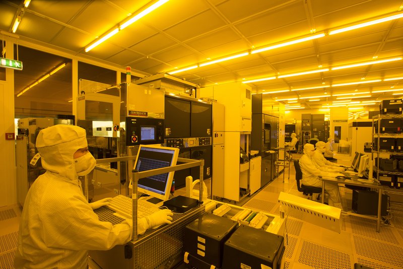
Clean room
24/7 R&D Pilot Line
The heart of the IHP is the state-of-the-art pilot line in a 1,500 m2 clean room, which is operated 24 hours/7 days a week. In addition, a further 300 m² of cleanroom space is available to enable wafer interconnects and heterointegration of chiplets.
The toolset enables 0.13-µm technology on 200-mm wafers. Cycle times are typically two days per lithography mask. Processing times from tape-in to shipping of diced chips are approximately 12 weeks, depending on the technology used.
Key wafer fabrication equipment within the pilot line includes:
- I-line and DUV (248 nm laser exposure) photolithography
- CMP in front-end of line (oxide, poly Si) and back-end of line (oxide, tungsten)
- dry etch processes for standard CMOS and BiCMOS process modules
- PVD (Co, Al, Ti, TiN, Ni) and CVD (W, TiN) for the Al metallization system
- Atomic-Layer-Deposition ALN for HfO2, Al2O, SiO2 and SiN
- PECVD (inclusive HDP) and SACVD for deposition of dielectrics in front-end of line and back-end of line
- wet etch and wet clean processes required for a technological level of 0.13 µm
- low temperature Si, SiGe, SiGe:C epitaxy (differential, and selective epitaxy)
- low to medium energy and low to high dose ion implantation (As, B, P, In, Sb, Si, Ge, F, Ar)
- oxidation, LPCVD (including low temperature oxide and nitride), and annealing in standard batch systems
- RTP for annealing, oxidation, and silicidation
- 8” high-vacuum bonding system
- 8” transfer printing toolset
- inline measurements for CD, overlay, thickness, resistance, defectivity, topology (SEM, AFM), and XRD
- parametric test using two fully automatic test systems
| Additional usable clean room area | 500 m² |
| Gross Floor Area | 3.800 m² |
| Gross Space Volume | 18.200 m³ |
| Length x width | 27 m x 35 m |
