Digital- and Mixed-Signal SoC Test Service

Facilities for Functional Test on Integrated Circuits

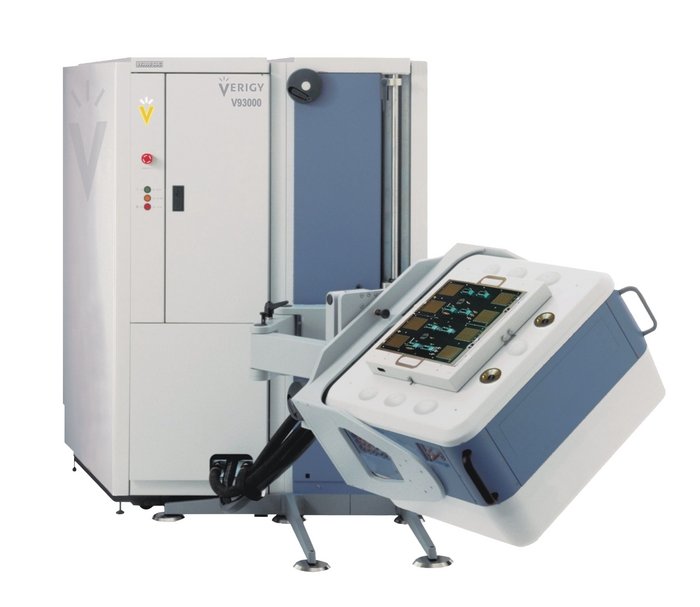
Production Test System - Advantest 93000

Power supply:
2xGP-DPS: 4 ch., max 16 A, ±8 V force/measure
MS-DPS: 8 ch., max 16 A, ±8 V force/measure
DPS32: 32 ch., max 48 A @ 3 V, 0-7 V force/measure
digital resources:
2xPS1600: 256 ch. @ 533 Mb/s, 32 ch. @ 1.6 Gb/s
1xPS9G: 64 ch. @ 800 Mb/s, 32 ch. @ 8 Gb/s
1xPSSL: 16 ch. @ 16 Gb/s

Analog resources:
MBAV8+: 
Source 4 AWG, max 200 MHz @ 500 Ms/s
Measure 4 Digitizers, max 16 bit @ 300 MHz
V-Source, PMU, HPPMU multiplex

Additional software for memory test and scan test analysis
Supports manual package test and automatic wafer test (using the UF200 wafer prober)

Accretech UF200 wafer prober
Fully automatic wafer prober for up to 25 wafers/lot
Supports 6inch and 8inch wafers
Temperature controlled chuck, -40°C up to +125°C

Prof. Miloš Krstić

Department Head

IHP 
Im Technologiepark 25
15236 Frankfurt (Oder)
Germany

Secretary:
Heike Wasgien
Phone: +49 335 5625 342
Fax: +49 335 5625 671 
Send e-mail »

Debugging Test System

MuTest

  • pre-series & medium scale
    volume production tester
  • radiation test
  • power supply
    • 8 channels with 800 mA
    • 2 channels with 5 A
    • Voltage range -4 V to 10 V
  • digital resources
    • 4xM-D864: 256 ch @ 800 Mb/s
    • voltage range -1.5 V to 6.5 V

Binder MK 53 E2

  • climate chamber for endurance tests
  • temperature range: 40 ° to 150 °C
  • fully programmable & remotely controllable

Thermostream TP04300

  • mobile programmable temperature system
  • temperature performance:
    • Range: -75 ° to 228 °C
    • Transition: ±180 °C in < 10 s
    • Accuracy: 1 °C
  • DUT temperature sensors

Infrared camera

Spectral range 7.5 .. 14µm
Temperature measurement range -40°C .. 1200°C
Image size 640x480

Standard lens 1.0/30 mm
image area (30 x 23)°,
minimum distance 300mm

Microscope objective 1,0x
image (16 x 12) mm²,
distance 50 mm, resolution 25µm

Online:
up to 10 points

Offline:
temperature of each pixel can be determined, additionally regions with min/max evaluation can be defined

Usage:
e.g. detection of hot spots on chips (caused by shorts), thermal check of PCBs, etc.

XT V 160 Electronics X-ray Inspection

Easy-to-use, cost-effective and high-quality PCB inspection system targeting production facilities and failure analysis laboratories.

  • Proprietary 160 kV source with submicron focal spot size
  • 1.45 Megapixel 12 bit camera with image enhancer
  • 5-axis manipulator (X,Y,Z, rotate, tilt)
  • 360° view
  • Real-time image display
  • Inspect X software

The website is designed for modern browsers. Please use a current browser.