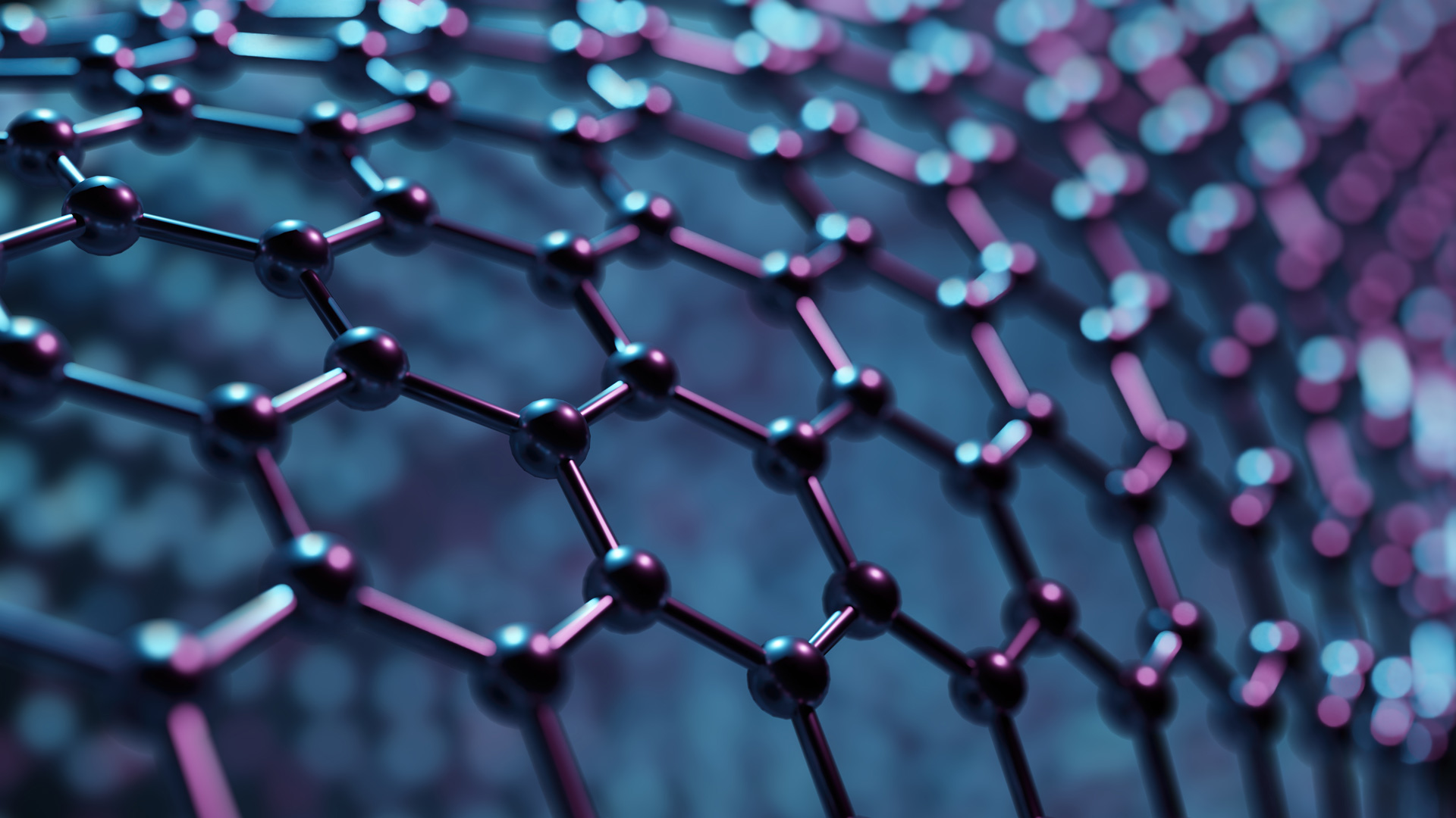
Der Fokus der Forschungsgruppe liegt auf dem Gebiet der Graphen- und hBN-Prozess- und Technologieentwicklung. Sie befasst sich sowohl mit grundlegenden Untersuchungen von Graphen und hBN als auch mit der Integration von neuartigen graphenbasierten Bauelementen in die Silizium-Technologieumgebung.
Einerseits ist es von größter Bedeutung, die morphologischen, kristallographischen, chemischen Eigenschaften und Wachstumsmechanismen von 2D-Materialien zu verstehen und zu kontrollieren. Andererseits werden die Entwicklungen von Graphenbauelementen auch unter Bedingungen durchgeführt, die der siliziumbasierten IC-Produktionsumgebung möglichst nahe kommen. Daher ist es unser Ziel, die Lücke zwischen der aktuellen Graphenforschung und modernsten 200-mm-CMOS-Technologien zu schließen. Eine erfolgreiche Zusammenarbeit zwischen den Abteilungen Materialforschung und Technologie sowie Kooperationen mit nationalen und europäischen Partnern sind etabliert, um die Ergebnisse der 2D-Materialforschung zu sichern.
Forschungsziele
- Forschung und Entwicklung von 2D-Materialien unter CMOS-kompatiblen Bedingungen
- Identifikation und Bewältigung der integrativen Herausforderungen der Graphentechnologie
- Design, Entwicklung und Herstellung von elektrooptischen Modulatoren, basierend auf Graphen
Forschungsschwerpunkte
- quantenmechanische Modellierung der Wachstumsmechanismen von Graphen und hBN
- Simulation und Modellierung der 2D-Bauelemente
- Entwicklung von 200-mm-CVD-Prozessen für hochwertiges Graphen und hBN
- physikalisches Verständnis der Substrat-Graphen-Grenzflächen
- Entwicklung von hBN/Graphen/HBN-Heterostrukturen
- erweiterte elektrische Charakterisierungen von 2D-Materialien
- Einsatz neuer Charakterisierungswerkzeuge und -methoden für die 2D-Materialanalyse
- Untersuchungen von Graphen-EA-Modulatoren und Graphen-Halbleiter-Dioden
- Entwicklung neuer Ansätze für die Herstellung von graphenbasierten Bauelementen
- Etablierung von 200-mm-generischen-Prozessen von Graphen in die CMOS-Pilotlinie
Forschungsergebnisse
Script list Publications
(1) Optimization of the Metal Deposition Process for the Accurate Estimation of Low Metal-Graphene Contact-Resistance
D. Capista, R. Lukose, F. Majnoon, M. Lisker, Ch. Wenger, M. Lukosius
Proc. 47th International ICT and Electronics Convention (MIPRO 2024), 1561 (2024)
DOI: 10.1109/MIPRO60963.2024.10569895, (2D-EPL)
(2) SWCNT-Si Photodetector with Voltage-Dependent Active Surface
D. Capista, L. Lozzi, A. Di Bartolomeo, F. Giubileo, N. Martucciello, M. Passacantando
Nano Express 5(1), 015004 (2024)
DOI: 10.1088/2632-959X/ad12d9
New works on Carbon Nanotubes-Silicon MIS heterostructures showed that the presence of thickness inhomogeneities in the insulating layer across the device can be exploited increase its functionalities. In this work, we report the fabrication and the characterization of a device consisting of a Single-Walled Carbon Nanotube (SWCNT) film onto an n-type silicon substrate where the nitride interlayer between the nanotubes and the silicon has been intentionally etched to obtain different thickness. Three different silicon nitride thicknesses allow the formation of three regions, inside the same device, each with different photocurrents and responsivity behaviors. We show that by selecting specific biases, the photoresponse of the regions can be switched on and off. This peculiar behavior allows the device to be used as a photodetector with a voltage dependent active surface. Scanning photo response imaging of the device surface, performed at different biases highlight this behavior.
(3) Advancing Graphene Integration in Si CMOS Technology: Challenges, Solutions, and Modulator Exploration
M. Lukosius, R. Lukose, P.K. Dubey, A.I. Raju, D. Capista, M. Lisker, A. Mai, Ch. Wenger
ECS Meeting Abstracts MA2024-02, 1455 (2024)
DOI: 10.1149/MA2024-02111455mtgabs, (2D-EPL)
(4) Graphene for Photonic Applications
M. Lukosius, R. Lukose, P.K. Dubey, A.I. Raju, M. Lisker, A. Mai, Ch. Wenger
Proc. 47th International ICT and Electronics Convention (MIPRO 2024), 1614 (2024)
DOI: 10.1109/MIPRO60963.2024.10569652, (2D-EPL)
(5) P-Type Schottky Contacts for Graphene Adjustable-Barriers Phototransistors
C. Strobel, C.A. Chavarin, M. Knaut, M. Albert, A. Heinzig, L. Gummadi, Ch. Wenger, T. Mikolajick
Nanomaterials (MDPI) 14(13), 1140 (2024)
DOI: 10.3390/nano14131140, (Graphen)
The graphene adjustable-barriers phototransistor is an attractive novel device for potential high speed and high responsivity dual-band photodetection. In this device graphene is embedded between the semiconductors silicon and germanium. Both n-type and p-type Schottky contacts between graphene and the semiconductors are required for this device. While n-type Schottky contacts are widely investigated, reports about p-type Schottky contacts between graphene and the two involved semiconductors are scarce. In this study, we demonstrate a p-type Schottky contact between graphene and p-germanium. A clear rectification with on-off ratios of close to 103 (± 5V) and a distinct photoresponse at telecommunication wavelengths in the infrared are achieved. Further, p-type silicon is transferred to or deposited on graphene and we also observe rectification and photoresponse in the visible range for some of these p-type Schottky junctions. These results are an important step towards a functional graphene adjustable-barriers phototransistor.
(6) High Gain Graphene Based Hot Electron Transistor with Record High Saturated Output Current Density
C. Strobel, C.A. Chavarin, M. Knaut, S. Völkel, M. Albert, A. Hiess, B. Max, Ch. Wenger, R. Kirchner, T. Mikolajick
Advanced Electronic Materials 10(2), 2300624 (2024)
DOI: 10.1002/aelm.202300624, (FFLEXCOM (D020))
Hot electron transistors (HETs) represent an exciting frontier in semiconductor technology, holding the promise of high-speed and high-frequency electronics. With the exploration of two-dimensional materials such as graphene and new device architectures, HETs are poised to revolutionize the landscape of modern electronics. This study highlights a novel HET structure with a record output current density of 800 A/cm² and a high current gain α, fabricated using a scalable fabrication approach. The HET structure comprises two-dimensional hexagonal boron nitride (hBN) and graphene layers wet transferred to a germanium substrate. The combination of these materials results in exceptional performance, particularly in terms of the highly saturated output current density. The scalable fabrication scheme used to produce the HET opens up opportunities for large-scale manufacturing. This breakthrough in HET technology holds promise for advanced electronic applications, offering high current capabilities in a practical and manufacturable device.