Diese Forschungsgruppe beschäftigt sich mit der Entwicklung von Funktionsmaterialien für die Mikroelektronik, die durch adaptive Implementierung in bereits existierende Si-basierte Technologien eine Vielfalt an Anwendungsgebiete und Herausforderungen der modernen Gesellschaft adressieren können. Durch die Gewinnung eines fundamentalen Verständnisses rund um die spezifischen Materialeigenschaften der Funktionsmaterialen, sowie der Erforschung innovativer Ansätze im Bereich ihrer Integration, des Bauteildesigns und der endgültigen systemischen Anwendung, bietet diese Forschungsrichtung potentielle und ausbaubare Lösungen im Rahmen des CMOS+X Kontextes an.
Um tiefergehendes Wissen zu erlangen, was zur präzisen Kontrolle der Eigenschaften dieser Materialsysteme und ihrer möglichen Integration erforderlich ist, nutzt unsere Gruppe synergetische Kompetenzen der theoretischen Modellierung in Kombination mit fortschrittlichen, hochmodernen experimentellen Techniken auf der Mikro- und Nanoskala.
Forschungsziele
- Weiterentwicklung, Charakterisierung und Modellierung von memristiven Bauelementen für nichtflüchtige Speicher, sowie deren Schaltungen und Algorithmen zur Anwendung in neuronalen Netzwerken und im Edge Computing
- Entwicklung und Integration von plasmonischen und dielektrischen Nahfeldsensoren des VIS/IR- und THz-Bereichs für hyperspektrale Bildgebung, medizinischen Diagnostik, Industrie-/Umweltmonitoring und Biofunktionalisierung
- Integration von III/V-Verbindungshalbleitermaterialien auf die etablierte CMOS-kompatible Siliziumtechnologieplattform für elektronische und photonische Bauelementkonzepte und -systeme
- Verständnis technologischer Probleme im Zusammenhang mit Defekten in Materialien und Bauelemente der Mikroelektronik und Photonik
Forschungsschwerpunkte
Die Diversität der Forschungsschwerpunkte und -themen in dieser Arbeitsgruppe verbildlicht das große Interesse, das immense Potential und die vielen Möglichkeiten, welche Funktionsmaterialien in der Verbesserung bereits existierende Technologien und in der Entwicklung neuer Bauteilkonzepte besitzen. Hierbei achten wir stets darauf, dass neue technologische Vorstöße in diesem Rahmen immer mit einer adaptiven Implementierung zu bereits etablierten Technologieplattformen vollzogen werden, um der Forschungsgemeinschaft und der Gesellschaft eine schnelle, effiziente und qualifizierte Bereitstellung unserer Lösungen zu ermöglichen.
Memristive Bauelemente weisen eine variable widerstandsbasierte Speicherfunktion auf. Von besonderem Interesse ist diese Art von Bauelementen als schaltbares Element für nichtflüchtige RRAM-Speicher, aber auch für den Bereich der analogen neuronalen Schaltungstechnik bzw. energieeffizientes In-Memory Computing. Hier eröffnen die memristiven Bauelemente die Möglichkeit, derzeitig bestehenden Hürden digitaler Datenverarbeitung im Bereich kognitiver Aufgabenstellungen zu überwinden. Im Mittelpunkt unseres Forschungsschwerpunktes „Neuronale Netzwerke“ steht die Entwicklung der memristiven Bauelemente auf Al:HfO2-Basis für zukünftige elektronische Schaltungen mit starker Orientierung an biologischen Systemen. Darauf aufbauend entwerfen wir KI-Lösungen als vielversprechendster Ansatz zur Beherrschung komplexer Aufgaben, wie etwa Bild-, Objekt- und Szenenerkennung, oder Regelung dynamischer, nichtlinearer Systeme für Anwendungsgebiete, wie z.B. E-Mobilität, Aerospace, Datenverarbeitung und Sensorkontrolle. Um die Funktionsfähigkeit von Memristive Bauelemente innerhalb eines intelligenten In-Memory-Computing-Konzepts unter extremen Umwelteinflüssen zu verstehen und am Ende auch zu gewährleisten, untersuchen wir ebenfalls die Auswirkungen von Strahlung und kyrogenischen Temperaturen auf unsere etablierten memristiven Bauelemente und ihre Systemarchitektur.
Die starke Evolution hin zu einer immer digitalisierten Gesellschaft und Industrie hat die Nachfrage nach modernen Sensorlösungen in neue Höhen steigen lassen. Im Mittelpunkt unseres Forschungsschwerpunktes „Sensorik“ steht die Entwicklung von plasmonischen, dielektrischen und photoakustischen Sensorsystemen für mannigfaltige Anwendungsbereichs des täglichen Lebens. Unter diese Prämisse untersuchen wir Biosensoren basierend auf Plasmonenresonanzen, welche zu den sensibelsten Methoden gehören, um Veränderungen der Ordnung eines einzelnen Biomoleküls nachzuweisen. Hierzu wurden kürzlich mit der BTU Cottbus-Senftenberg die ersten plasmonischen Sensoren entwickelt und getestet, um Krankheiten von Nutzpflanzen frühzeitig erkennen zu können. Die Energiewende in der Lausitz-Region wandelt das traditionelle Kohlerevier zur Modellregion der Wasserstoffstrategie, wobei (Kohlen-)Wasserstoffe (synthetische Kraftstoffe) als wichtige Energieträger der Zukunft für stationäre und mobile Anwendungen gelten. Um den einhergehenden enormer Bedarf an leistungsfähigen Sensoren für die sicherheitsrelevante Überwachung der fluiden Kraftstoffe zu bedienen, beteiligen wir uns im Rahmen des Projektes iCampms 2.0 an der Entwicklung moderner dielektrischer (Kohlen-)wasserstoff-Sensoren. Des Weiteren engagieren wir uns im ebenfalls an der BTU Cottbus-Senftenberg lokalisierten BMBF-Verbundvorhaben OASYS an der Entwicklung von metaoberflächen-basierten dielektrischen Nahfeldsensoren für eine Vielzahl innovativer Anwendungen z.B. im Bereich der hyperspektrale Bildgebung, medizinischen Diagnostik, aber auch der industriellen Fertigung und modernen Agrar-/Umweltwirtschaft.
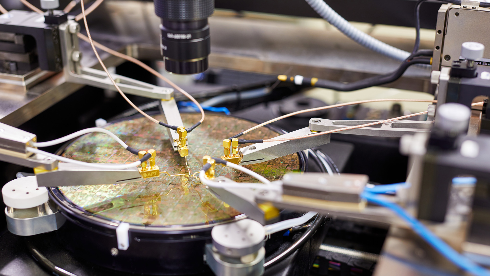
Die kontinuierliche Skalierung und Entwicklung von rein Silizium-basierten mikroelektronischen Bauelementen erreicht mehr und mehr ihre Grenzen. Verbindungshalbleiter der Gruppe III/V haben sich mittlerweile als vielversprechende Kandidaten herauskristallisiert, aufgrund ihrer überlegenen Eigenschaften (bei z.B. Ladungsträgerbeweglichkeit und der Fähigkeit, Bandlücken zu erzeugen), diese Grenzen zu überwinden. Dies macht die III/V-Verbindungshalbleiter interessant sowohl für den Einsatz in elektronischen Bauteilen, als auch in aktiven photonischen Bauelementen und in der Quantentechnologie. Im Mittelpunkt unseres Forschungsschwerpunktes „III/V-on-Si“ steht eine angestrebte Ko-Integration von III/V-Materialien auf-Silizium, um hochleistungsfähige, kostengünstige Systeme zu ermöglichen, welche die vorteilhaften III/V-Eigenschaften und -Funktionen mit der ausgereiften Mainstream-Silizium-Fertigungstechnologie kombinieren. In diesem Rahmen sind wir bestrebt, III/V-Materialien, Prozesse und Bauelemente in der neuen, von der FMD-finanzierten Versuchsprozesslinie im Reinraum für die künftige Umsetzung in einem CMOS+X-kompatiblen Kontext zu erforschen.
Forschungsergebnisse
Script list Publications
A. Blumenstein, E. Perez, Ch. Wenger, N. Dersch, A. Kloes, B. Iniguez, M. Schwarz
Solid-State Electronics 232, 109296 (2026)
DOI: 10.1016/j.sse.2025.109296
This paper investigates the impact of introducing variability to trained neural networks and examines the effects of variability and quantization on network accuracy. The study utilizes the MNIST dataset to evaluate various Multi-Layer Perceptron configurations: a baseline model with a Single-Layer Perceptron and an extended model with multiple hidden nodes. The effects of Cycle-to-Cycle variability on network accuracy are explored by varying parameters such as the standard deviation to simulate dynamic changes in network weights. In particular, the performance differences between the Single-Layer Perceptron and the Multi-Layer Perceptron with hidden layers are analyzed, highlighting the network’s robustness to stochastic perturbations. These results provide insights into the effects of quantization and network architecture on accuracy under varying levels of variability.
(2) Deposition of CeOx/SnOx-Based Thin Films via RF Magnetron Sputtering for Resistive Gas Sensing Applications
A. Kalra, C.A. Chavarin, P. Nitsch, R. Tschammer, J.I. Flege, M. Ratzke, M.H. Zoellner, M.A. Schubert, Ch. Wenger, I.A. Fischer
Physica B: Condensed Matter 723, 418098 (2026)
DOI: 10.1016/j.physb.2025.418098, (iCampus II)
Cerium oxide-tin oxide (CeOx/SnOx) thin films with varying Sn content were deposited using RF magnetron sputtering and investigated for hydrogen sensing applications. Structural, compositional and morphological properties were characterized using X-ray diffraction (XRD), X-ray photoelectron spectroscopy (XPS), atomic force microscopy (AFM), transmission electron microscopy (TEM) and energy-dispersive X-ray spectroscopy (EDX). Gas sensing measurements showed effective hydrogen detection at room temperature, with the sensitivity strongly influenced by Sn content and oxygen vacancy concentration. Higher Sn concentration enhanced the sensing response, which was correlated with microstructural features obtained from AFM and EDX, as well as with the presence of Ce3+ and Ce4+ oxidation states identified by XPS. This study highlights the potential of CeOx/SnOx thin films for possible back-end-of-line integration and provides proof-of-principle for room-temperature hydrogen sensing.
(3) Variability in HfO2-based Memristors under Pulse Operation
D. Maldonado, C. Acal, H. Ortiz, F. Navas-Gomez, A. Cantudo, Ch. Wenger, E. Pérez, J.B. Roldán
Microelectronic Engineering 304, 112445 (2026)
DOI: 10.1016/j.mee.2026.112445, (AVMMSafe)
We have studied device-to-device variability in TiN/Ti/HfO2/TiN devices under pulse operation. We measured extensively memristive devices that are CMOS integrated with different pulse trains, changing the pulse width and amplitude for groups of more than one hundred devices. The statistical parameters of the measured current were extracted to better understand the device physics under the pulse operation regime. An analytical model to describe synaptic depression and potentiation behavior in the device conductance is introduced, it fits accurately the means of the current data for all the pulse trains under study. In addition, an explanation of the measurements is enlightened with kinetic Monte Carlo simulations that allow the study of resistive switching at the atomic level. Finally, the probability distribution functions of the measured currents in some of the pulses within the pulse series employed are analyzed to extract the probability distribution that works better. A proposal for the implementation of device-to-device variability in the Stanford models is introduced.
(1) Strategien für wellenlängenselektive Ge-Photodetektoren in 200-mm-Wafer-Siliziumtechnologie
L. Augel, S. Reiter, A. Sengül, Ch. Mai, C.A. Chavarin, P. Oleynik, F. Berkmann, Ch. Wenger, I.A. Fischer
Proc. 11. MikroSystemTechnik Kongress (MST 2025), 180 (2025)
(iCampus II)
(2) Enhancing RRAM Reliability: Exploring the Effects of Al Doping on HfO2-Based Devices
A. Baroni, E. Pérez, K.D.S. Reddy, S. Pechmann, Ch. Wenger, D. Ielmini, C. Zambelli
IEEE Transactions on Device and Materials Reliability 25(3), 379 (2025)
DOI: 10.1109/TDMR.2025.3581061
This study provides a comprehensive evaluation of RRAM devices based on HfO2 and Al-doped HfO2 insulators, focusing on critical performance metrics, including Forming yield, Post-Programming Stability (PPS), Fast Drift, Endurance, and Retention at elevated temperatures (125 ∘C). Aluminum doping significantly enhances device reliability and stability, improving Forming yield, reducing current drift during programming and Retention tests, and minimizing variability during Endurance cycling. While Al5%:HfO2 achieves most of the observed benefits compared to pure HfO2, Al7%:HfO2 offers incremental advantages for scenarios requiring extreme reliability. These findings position Al-doped HfO2 devices as a promising solution for RRAM-based systems in memory and neuromorphic computing, highlighting the potential trade-off between performance gains and increased fabrication complexity. This work underlines the importance of material engineering for optimizing RRAM devices in application-specific contexts.
(3) Comparing Short and Long-Term Reliability of HfO2 and Al:HfO2 RRAM Devices
A. Baroni, E. Pérez, K.D.S. Reddy, S. Pechmann, Ch. Wenger, D. Ielmini, C. Zambelli
Proc. IEEE International Integrated Reliability Workshop (IIRW 2024), (2025)
DOI: 10.1109/IIRW62856.2024.10947134
(4) On-Chip-Brechungsindex-Sensoren in 200-mm-Wafer-Siliziumtechnologie
F. Berkmann, S. Reiter, A. Sengül, Ch. Mai, C.A. Chavarin, Ch. Wenger, I.A. Fischer
Proc. 11. MikroSystemTechnik Kongress (MST 2025), 476 (2025)
(iCampus II)
(5) Evaluating Device Variability in RRAM-Based Single and Multi-Layer Perceptrons
A. Blumenstein, E. Perez, Ch. Wenger, N. Dersch, A. Kloes, B. Iniguez, M. Schwarz
Proc. 32nd International Conference Mixed Design of Integrated Circuits and Systems (MIXDES 2025), abstr. book 33 (2025)
(AVMMSafe)
(6) Evaluating Device Variability in RRAM-Based Single- and Multi-Layer Perceptrons
A. Blumenstein, E. Perez, Ch. Wenger, N. Dersch, A. Kloes, B. Iniguez, M. Schwarz
Proc. 32nd International Conference Mixed Design of Integrated Circuits and Systems (MIXDES 2025), 74 (2025)
DOI: 10.23919/MIXDES66264.2025.11092102, (AVMMSafe)
(7) CMOS-Compatible Ge Metasurface Nanostructures with FTIR-Validated Resonance Optimization
W.-H. Chen, J. Schlipf, G. Capellini, P. Oleynik, D. Ryzhak, Y. Yamamoto, W.-C. Wen, K. Hnida-Gut, Ch. Wenger, I.A. Fischer, O. Skibitzki
Proc. 10th International Symposium on Control of Semiconductor Interfaces (ISCSI-X), the International Conference on Silicon Epitaxy and International SiGe Technology and Device Meeting (ICSI/ISTDM 2025), 205 (2025)
(OASYS)
(8) CW Electrically Pumped GeSn/SiGeSn MQW Lasers
O. Concepción, L. Seidel, T. Liu, G. Capellini, M. Oehme, D. Grützmacher, D. Buca
Proc. IEEE Silicon Photonics Conference (SiPhotonics 2025), ThB6 (2025)
DOI: 10.1109/SiPhotonics64386.2025.10985491
(9) Statistical Model for the Calculation of Conductance Variations of Memristive Devices
N. Dersch, E. Perez, Ch. Wenger, M. Lanza, K. Zhu, M. Schwarz, B. Iniguez, A. Kloes
Proc. 51st IEEE European Solid-State Electronics Research Conference (ESSERC 2025), 373 (2025)
DOI: 10.1109/ESSERC66193.2025.11213973, (AVMMSafe)
(10) A Closed-Form Model for Programming of Oxide-Based Resistive Random Access Memory Cells Derived From the Stanford Model
N. Dersch, E. Perez, Ch. Wenger, M. Schwarz, B. Iniguez, A. Kloes
Solid-State Electronics 230, 109238 (2025)
DOI: 10.1016/j.sse.2025.109238
This paper presents a closed-form model for pulse-based programming of oxide-based resistive random access memory devices. The Stanford model is used as a basis and solved in a closed-form for the programming cycle. A constant temperature is set for this solution. With the closed-form model, the state of the device after programming or the required programming settings for achieving a specific device conductance can be calculated directly and quickly. The Stanford model requires time-consuming iterative calculations for high accuracy in transient analysis, which is not necessary for the closed-form model. The closed-form model is scalable across different programming pulse widths and voltages.
(11) Performance of Pulse-Programmed Memristive Crossbar Array with Bimodally Distributed Stochastic Synaptic Weights
N. Dersch, E. Perez, Ch. Wenger, Ch. Roemer, M. Schwarz, B. Iniguez, A. Kloes
Solid-State Electronics 227, 109128 (2025)
DOI: 10.1016/j.sse.2025.109128, (KI-IoT)
In this paper, we present a method of implementing memristive crossbar arrays with bimodally distributed weights. The bimodal distribution is a result of pulse-based programming. The memristive devices are used for implementing synaptic weights and can only have an ON (logical “1″) or an OFF (logical ”0″) state. The state of the memristive device after programming is determined by the bimodal distribution. The highly efficient noise-based variability approach is used to simulate this stochasticity. The memristive crossbar array is used to classify the MNIST data set and comprises more than 15,000 weights. The interpretation of these weights is investigated. In addition, the influence of the stochasticity of the weights and the accuracy of the weights on the classification results is considered and various programming settings are examined.
(12) CSiGeSn Epitaxy: Future Isovalent Isomorphism in Group-IV Materials
A.J. Devaiya, O. Concepcion, T. Fischer, A. Tiedemann, G. Capellini, S. Mathur, D. Grützmacher, D. Buca
Proc. 16th International Workshop on New Group IV Semiconductor Nanoelectronics (El4GroupIV 2025), 35 (2025)
(13) RISC-V CPU Design using RRAM-CMOS Standard Cells
M. Fritscher, M. Uhlmann, P. Ostrovskyy, D. Reiser, J.-C. Chen, J. Wen, C. Schulze, G. Kahmen, D. Fey, M. Reichenbach, M. Krstic, Ch. Wenger
IEEE Transactions on Very Large Scale Integration (VLSI) Systems 33(9), 2406 (2025)
DOI: 10.1109/TVLSI.2025.3554476, (iCampus II)
The breakdown of Dennard scaling has been the driver for many innovations such as multicore CPUs and has fueled the research into novel devices such as resistive random access memory (RRAM). These devices might be a means to extend the scalability of integrated circuits since they allow for fast and nonvolatile operation. Unfortunately, large analog circuits need to be designed and integrated in order to benefit from these cells, hindering the implementation of large systems. This work elaborates on a novel solution, namely creating digital standard cells utilizing RRAM devices. Albeit this approach can be used both for small gates and large macroblocks we illustrate it for a 2T2R-cell. Since RRAM devices can be vertically stacked with transistors this enables us to construct a NAND standard cell which merely consumes the area of two transistors. This leads to a 25% area reduction compared to an equivalent CMOS NAND gate. We illustrate achievable area savings with a halfadder circuit and integrate this novel cell into a digital standard cell library. A synthesized RISC-V core using RRAM-based cells results in a 10.7% smaller area than the equivalent design using standard CMOS gates.
(14) RISC-V CPU Design using RRAM-CMOS Standard Cells
M. Fritscher, M. Uhlmann, P. Ostrovskyy, D. Reiser, J.-C. Chen, J. Wen, C. Schulze, G. Kahmen, D. Fey, M. Reichenbach, M. Krstic, Ch. Wenger
IEEE Transactions on Very Large Scale Integration (VLSI) Systems 33(9), 2406 (2025)
DOI: 10.1109/TVLSI.2025.3554476, (6G-RIC)
The breakdown of Dennard scaling has been the driver for many innovations such as multicore CPUs and has fueled the research into novel devices such as resistive random access memory (RRAM). These devices might be a means to extend the scalability of integrated circuits since they allow for fast and nonvolatile operation. Unfortunately, large analog circuits need to be designed and integrated in order to benefit from these cells, hindering the implementation of large systems. This work elaborates on a novel solution, namely creating digital standard cells utilizing RRAM devices. Albeit this approach can be used both for small gates and large macroblocks we illustrate it for a 2T2R-cell. Since RRAM devices can be vertically stacked with transistors this enables us to construct a NAND standard cell which merely consumes the area of two transistors. This leads to a 25% area reduction compared to an equivalent CMOS NAND gate. We illustrate achievable area savings with a halfadder circuit and integrate this novel cell into a digital standard cell library. A synthesized RISC-V core using RRAM-based cells results in a 10.7% smaller area than the equivalent design using standard CMOS gates.
(15) RISC-V CPU Design using RRAM-CMOS Standard Cells
M. Fritscher, M. Uhlmann, P. Ostrovskyy, D. Reiser, J.-C. Chen, J. Wen, C. Schulze, G. Kahmen, D. Fey, M. Reichenbach, M. Krstic, Ch. Wenger
IEEE Transactions on Very Large Scale Integration (VLSI) Systems 33(9), 2406 (2025)
DOI: 10.1109/TVLSI.2025.3554476, (HYB-RISC)
The breakdown of Dennard scaling has been the driver for many innovations such as multicore CPUs and has fueled the research into novel devices such as resistive random access memory (RRAM). These devices might be a means to extend the scalability of integrated circuits since they allow for fast and nonvolatile operation. Unfortunately, large analog circuits need to be designed and integrated in order to benefit from these cells, hindering the implementation of large systems. This work elaborates on a novel solution, namely creating digital standard cells utilizing RRAM devices. Albeit this approach can be used both for small gates and large macroblocks we illustrate it for a 2T2R-cell. Since RRAM devices can be vertically stacked with transistors this enables us to construct a NAND standard cell which merely consumes the area of two transistors. This leads to a 25% area reduction compared to an equivalent CMOS NAND gate. We illustrate achievable area savings with a halfadder circuit and integrate this novel cell into a digital standard cell library. A synthesized RISC-V core using RRAM-based cells results in a 10.7% smaller area than the equivalent design using standard CMOS gates.
(16) Sensing of Hemin Binding to Albumin using Ge-based Plasmonic Antennas Operating in the THz Range
E. Hardt, R. Varricchio, C.A. Chavarin, G. De Simone, O. Skibitzki, P. Ascenzi, A. di Masi, G. Capellini
IEEE Sensors Journal 25(8), 12881 (2025)
DOI: 10.1109/JSEN.2025.3545736, (IHP- Roma Tre University Joint Lab)
Albumin-based biofunctionalized biosensors have the potential to be utilized for the detection of physiological ligands (e.g., heme) and of pathogenic proteins. In human cells, heme is always bound to proteins due to its toxic nature. However, free heme can be present within tissue and in the bloodstream as a consequence of hemolysis or under pathological conditions like malaria or sickle cell anemia. Therefore, the development of an albumin-based heme biosensor could be relevant from a biomedical viewpoint. In this study, we developed a protein-sensing platform by immobilizing albumin on CMOS-compatible Ge-based THz plasmonic antennas via drop-cast biofunctionalization. To set up the biosensor, the sensing platform was used to quantitatively measure the binding of hemin, a well-known physiological ligand of albumin. This measurement was performed using THz time-domain spectroscopy in dichroic transmission mode, achieving a sensitivity of approximately ~ 200 GHz/mM of the HSA:hemin complex. These preliminary results support the use of CMOS-compatible Ge-based THz plasmonic antennas as innovative sensors that could be monolithically integrated with conventional electronics for storage, processing, and communication into an all-in-one system.
(17) Sensing of Hemin Binding to Albumin using Ge-based Plasmonic Antennas Operating in the THz Range
E. Hardt, R. Varricchio, C.A. Chavarin, G. De Simone, O. Skibitzki, P. Ascenzi, A. di Masi, G. Capellini
IEEE Sensors Journal 25(8), 12881 (2025)
DOI: 10.1109/JSEN.2025.3545736, (iCampus II)
Albumin-based biofunctionalized biosensors have the potential to be utilized for the detection of physiological ligands (e.g., heme) and of pathogenic proteins. In human cells, heme is always bound to proteins due to its toxic nature. However, free heme can be present within tissue and in the bloodstream as a consequence of hemolysis or under pathological conditions like malaria or sickle cell anemia. Therefore, the development of an albumin-based heme biosensor could be relevant from a biomedical viewpoint. In this study, we developed a protein-sensing platform by immobilizing albumin on CMOS-compatible Ge-based THz plasmonic antennas via drop-cast biofunctionalization. To set up the biosensor, the sensing platform was used to quantitatively measure the binding of hemin, a well-known physiological ligand of albumin. This measurement was performed using THz time-domain spectroscopy in dichroic transmission mode, achieving a sensitivity of approximately ~ 200 GHz/mM of the HSA:hemin complex. These preliminary results support the use of CMOS-compatible Ge-based THz plasmonic antennas as innovative sensors that could be monolithically integrated with conventional electronics for storage, processing, and communication into an all-in-one system.
(18) Broadband Light Emission from GaAsP and GaInP Islands Grown on Silicon Nanotips Wafer via Nanoheteroepitaxy
N. Kafi, A. Rodrigues, I. Häusler, H. Ma, C. Netzel, A. Hammud, O. Skibitzki, M. Schmidbauer, F. Hatami
Applied Physics Letters 127(19), 191106 (2025)
DOI: 10.1063/5.0285546, (NHEQuanLEA)
We present the monolithic integration of GaAsxP1−x and GaxIn1−xP islands, selectively grown on a Si(001) nanotip wafer using gas-source molecular-beam epitaxy via a nanoheteroepitaxy approach. Optimal growth temperatures balancing selectivity and compositional control are 520–580 °C for GaAsP and 500–510 °C for GaInP. By adjusting the group III and V fluxes, island luminescence is tuned across a broad spectral range from 1.5 to 2.1 eV. High-resolution x-ray diffraction measurements on ensembles exceeding one million islands confirm that both GaAsP and GaInP islands are relaxed, while broad diffraction linewidths point to alloy fluctuations. Scanning transmission electron microscopy combined with energy-dispersive x-ray spectroscopy reveals compositional variations of up to 6% among the GaAsP islands, with nearly uniform composition within individual islands. In the case of GaInP, indium-rich regions are observed within single islands, with up to 11% variation across the ensemble. These compositional variations result in broadened or multiple luminescence peaks. Despite challenges in achieving full uniformity, this work demonstrates an alternative pathway for the monolithic integration of scalable III–V infrared-to-visible light emitters and detectors on silicon, advancing the development of microscale light sources for the silicon platform.
(19) Character Recognition Application of a Neural Circuit Including Lateral Inhibitory Mechanisms
D. Llobet Muñoz, I.K. Chatzipaschalis, A. Calomarde, A. Rubio
Proc. 40th Conference on Design of Circuits and Integrated Systems (DCIS 2025), 108 (2025)
DOI: 10.1109/DCIS67520.2025.11281935
(20) A Comprehensive Statistical Study of the Post-Programming Conductance Drift in HfO2-based Memristive Devices
D. Maldonado, C. Acal, H. Ortiz, A.M. Aguilera, J.E. Ruiz-Castro, A. Cantudo, A. Baroni, K.D.S. Reddy, S. Pechmann, M. Uhlmann, Ch. Wenger, E. Perez, J.B. Roldan
Materials Science in Semiconductor Processing 196, 109668 (2025)
DOI: 10.1016/j.mssp.2025.109668, (KI-IoT)
(21) Effects of the Compliance Current on the Switching of HfO2 and Al:HfO2 Memristive Devices: Characterization and Modeling
D. Maldonado, K.D.S. Reddy, S. Pechmann, Ch. Wenger, J.B. Roldán, E. Pérez
Proc. 15th Spanish Conference on Electron Devices (CDE 2025), (2025)
DOI: 10.1109/CDE66381.2025.11038898, (KI-IoT)
(22) A Statistical and Modeling Study on the Effects of Radiation on Au/Ta/ZrO2(Y)/Pt/Ti Memristive Devices
D. Maldonado, A. Cantudo, D.V. Guseinov, M.N. Koryazhkina, E.V. Okulich, D.I. Tetelbaum, N.O. Bartev, N.G. Danchenko, V.A. Pikar, A.V. Teterevkov, F. Jiménez-Molinos, A.N. Mikhaylov, J.B. Roldán
Chaos, Solitons & Fractals 191, 115909 (2025)
DOI: 10.1016/j.chaos.2024.115909
In this study we have investigated the impact of radiation on the performance and reliability of Au/Ta/ZrO2(Y)/Pt/Ti memristive devices, with a particular focus on understanding the changes induced by ion irradiation. A comprehensive experimental approach was employed, involving irradiation with various ion species, including H⁺, Ne⁺, O⁺, and Kr⁺ to simulate different radiation environments. Thus, advanced statistical and modeling techniques to analyze the effects of irradiation on the resistive switching (RS) characteristics of the devices have been employed. Results revealed significant alterations in the RS parameters post-irradiation, including set and reset voltages and currents. These changes were found to vary depending on the ion species and dosage, with heavier ions such as Kr⁺ causing more pronounced effects. The findings are supported by detailed Monte Carlo simulations, which provided insights into the distribution of vacancies within the memristive devices under neutron irradiation. The experimental data, combined with the modeling results, indicate that ion irradiation can lead to the formation of defect structures that critically affect the performance of memristive devices.
(23) Dependable Neuromorphic Computing-in-Memory Architectures
F. Merchant, A. Bende, M. Fritscher, S. Kvatinsky, S. Singh, V. Rana, R. Dittmann, K.D.S. Reddy, Ch. Wenger, F. Mir, M. Taouil, M. Dev Gomony, S. Hamdioui, H. Corporaal
Proc. 30th IEEE European Test Symposium (ETS 2025), (2025)
DOI: 10.1109/ETS63895.2025.11049617, (HYB-RISC)
(24) Hydrogen Sensing via Heterolytic H2 Activation at Room Temperature by Atomic Layer Deposited Ceria
C. Morales, R. Tschammer, E. Pozarowska, J. Kosto, I.J. Villar-Garcia, V. Pérez-Dieste, M. Favaro, D. Starr, P. Kapuscik, M. Mazur, D. Wojcieszak, J. Domaradzki, C.A. Chavarin, Ch. Wenger, K. Henkel, J.I. Flege
ChemSusChem 18(13), e202402342 (2025)
DOI: 10.1002/cssc.202402342, (iCampus II)
Ultrathin atomic layer deposited ceria films (< 20 nm) are capable of H2 heterolytic activation at room temperature, undergoing a significant reduction regardless of the absolute pressure, as measured under in-situ conditions by near ambient pressure X-ray photoelectron spectroscopy. ALD-ceria can gradually reduce as a function of H2 concentration under H2/O2 environments, especially for diluted mixtures below 10%. At room temperature, this reduction is limited to the surface region, where the hydroxylation of the ceria surface induces a charge transfer towards the ceria matrix, reducing Ce4+ cations to Ce3+. Thus, ALD-ceria replicates the expected sensing mechanism of metal oxides at low temperatures without using any noble metal decorating the oxide surface to enhance H2 dissociation. The intrinsic defects of the ALD deposit seem to play a crucial role since the post-annealing process capable of healing these defects leads to decreased film reactivity. The sensing behavior was successfully demonstrated in sensor test structures by resistance changes towards low concentrations of H2 at low operating temperatures without using noble metals. These promising results call for combining ALD-ceria with more conductive metal oxides, taking advantage of the charge transfer at the interface and thus modifying the depletion layer formed at the heterojunction.
(25) Bottom-Up Strategy to Develop Ultrathin Active Layers by Atomic Layer Deposition for Room Temperature Hydrogen Sensors
C. Morales, R. Tschammer, D. Guttmann, K. Henkel, J.I. Flege, C. Ruffert, C.A. Chavarin, Ch. Wenger,
Proc. 11. MikroSystemTechnik Kongress (MST 2025), 71 (2025)
(iCampus II)
(26) In Situ X-Ray Photoelectron Spectroscopy Study of Atomic Layer Deposited Cerium Oxide on SiO2: Substrate Influence on the Reaction Mechanism During the Early Stages of Growth
C. Morales, M. Gertig, M. Kot, C.A. Chavarin, M.A. Schubert, M.H. Zoellner, Ch. Wenger, K. Henkel, J.I. Flege
Advanced Materials Interfaces 12(5), 2400537 (2024)
DOI: 10.1002/admi.202400537, (iCampus II)
Thermal atomic layer deposition (ALD) of cerium oxide using commercial Ce(thd)4 precursor and O3 on SiO2 substrates is studied employing in-situ X-ray photoelectron spectroscopy (XPS). The system presents a complex growth behavior determined by the change in the reaction mechanism when the precursor interacts with the substrate or the cerium oxide surface. During the first growth stage, non-ALD side reactions promoted by the substrate affect the growth per cycle, the amount of carbon residue on the surface, and the oxidation degree of cerium oxide. On the contrary, the second growth stage is characterized by a constant growth per cycle in good agreement with the literature, low carbon residues, and almost fully oxidized cerium oxide films. This distinction between two growth regimes is not unique to the CeOx/SiO2 system but can be generalized to other metal oxide substrates. Furthermore, the film growth deviates from the ideal layer-by-layer mode, forming micrometric inhomogeneous and defective flakes that eventually coalesce for deposit thicknesses above 10 nm. The ALD-cerium oxide films present less order and a higher density of defects than films grown by physical vapor deposition techniques, likely affecting their reactivity in oxidizing and reducing conditions.
(27) Effects of Temperature and Light on CeO2/SnO2 Thin-Film Hydrogen Sensors
A. Mudundi, A. Kalra, R. Tschammer, C. Morales, J.I. Flege, I.A. Fischer, C.A. Chavarin, Ch. Wenger
Proc. 11. MikroSystemTechnik Kongress (MST 2025), 20 (2025)
(iCampus II)
(28) Cryogenic Characterization of HfO₂-Based RRAM: Exploring Multilevel Switching from 300 K to 1.5 K for Neuromorphic Quantum Computing
E. Perez-Bosch Quesada, A. Mistroni, R. Jia, K.D.S. Reddy, M. Fritscher, F. Reichmann, H. Castan, S. Dueñas, Ch. Wenger, E. Perez
Proc. 57th International Conference on Solid State Devices and Materials (SSDM 2025), 703 (2025)
(INSEKT)
(29) Impact of the Series Resistance on Switching Characteristics of 1T1R HfO2-based RRAM Devices
E. Perez, D. Maldonado, S. Pechmann, K.D.S. Reddy, M. Uhlmann, A. Hagelauer, J.B. Roldan, Ch. Wenger
Proc. 15th Spanish Conference on Electron Devices (CDE 2025), (2025)
DOI: 10.1109/CDE66381.2025.11038868, (KI-IoT)
(30) Analytical Model for Parasitic Resistances of Crossbar Arrays Suitable for Open-Loop Programming Schemes Reliability Analysis
T. Rizzi, T. Zanotti, N. Lepri, E. Pérez, F.M. Puglisi, D. Ielmini, C. Zambelli
Proc. IEEE International Integrated Reliability Workshop (IIRW 2024), (2025)
DOI: 10.1109/IIRW62856.2024.10947147, (HYB-RISC)
(31) Monolithically Integrated GaAs Nanoislands on CMOS-Compatible Si Nanotips using GS-MBE
A. Rodrigues, A. Kamath, H. Illner, N. Kafi, O. Skibitzki, M. Schmidbauer, F. Hatami
Nanomaterials (MDPI) 15(14), 1083 (2025)
DOI: 10.3390/nano15141083, (NHEQuanLEA)
The monolithic integration of III-V semiconductors with silicon (Si) is a critical step toward advancing optoelectronic and photonic devices. In this work, we present GaAs nanoheteroepitaxy (NHE) on Si nanotips using gas-source molecular beam epitaxy (GS-MBE). We discuss the selective growth of fully relaxed GaAs nanoislands on complementary metal oxide semiconductor (CMOS)-compatible Si(001) nanotip wafers. Nanotip wafers were fabricated using a state-of-the-art 0.13 μm SiGe Bipolar CMOS pilot line on 200 mm wafers. Our investigation focuses on understanding the influence of the growth conditions on the morphology, crystalline structure, and defect formation of the GaAs islands. The morphological, structural, and optical properties of the GaAs islands were characterized using scanning electron microscopy, high-resolution X-ray diffraction, and photoluminescence spectroscopy. For samples with less deposition, the GaAs islands exhibit a monomodal size distribution, with an average effective diameter ranging between 100 and 280 nm. These islands display four distinct facet orientations corresponding to the {001} planes. As the deposition increases, larger islands with multiple crystallographic facets emerge, accompanied by a transition from a monomodal to a bimodal growth mode. Single twinning is observed in all samples. However, with increasing deposition, not only a bimodal size distribution occurs, but also the volume fraction of the twinned material increases significantly. These findings shed light on the growth dynamics of nanoheteroepitaxial GaAs and contribute to ongoing efforts toward CMOS-compatible Si-based nanophotonic technologies.
(32) Investigation of Dislocations Introduced in Si Wafer During Flash Lamp Annealing by Photoluminescence Spectroscopy
D. Ryzhak, G. Kissinger, A. Ehlert, A. Sattler, D. Spirito, D. Kot
Physica Status Solidi A 222(8), 2400753 (2025)
DOI: 10.1002/pssa.202400753, (Siltronic Project)
Dislocations are generated in Si wafers during flash lamp annealing for 20 ms. The samples have been etched to different depths and macro-photoluminescence (PL) spectra have been recorded for different dislocation densities. A micro-PL investigation is also carried out on a cross section of a sample. Four characteristic emission peaks are found, which are the well-known D1, D2, D3, and D4 lines. The findings demonstrate a significant influence of the defect densities on the PL spectra of the D lines by using both the micro- and the macro-PL setups, and show a correlation of the PL intensities with etch pit density measured against the depth of the wafer. Additionally, the D lines dependency on temperature is explored, offering insights into the underlying mechanisms. The D lines exhibit a pronounced temperature dependence, which can be attributed to various factors including phonon interactions and thermal expansion effects. The influence of nickel contamination is also examined.
(33) Photoluminescence Enhancement in Germanium All-Dielectric Metasurfaces
J. Schlipf, D. Ryzhak, P. Oleynik, G. Capellini, Y. Yamamoto, O. Skibitzki, I.A. Fischer
Proc. 10th International Symposium on Control of Semiconductor Interfaces (ISCSI-X), the International Conference on Silicon Epitaxy and International SiGe Technology and Device Meeting (ICSI/ISTDM 2025), 177 (2025)
(OASYS)
(34) Photoluminescence Enhancement in Germanium All-Dielectric Metasurfaces
J. Schlipf, D. Ryzhak, P. Oleynik, G. Capellini, Y. Yamamoto, O. Skibitzki, I.A. Fischer
Proc. 10th International Symposium on Control of Semiconductor Interfaces (ISCSI-X), the International Conference on Silicon Epitaxy and International SiGe Technology and Device Meeting (ICSI/ISTDM 2025), 177 (2025)
(iCampus II)
(35) AI-Driven Model for Optimized Pulse Programming of Memristive Devices
B. Spetzler, M. Fritscher, S. Park, N. Kim, Ch. Wenger, M. Ziegler
APL Machine Learning 3(2), 026103 (2025)
DOI: 10.1063/5.0251113, (DI-SIGN-HEP)
Next-generation artificial intelligence (AI) hardware based on memristive devices offers a promising approach to reducing the increasingly large energy consumption of AI applications. However, programming memristive AI hardware to achieve a desired synaptic weight configuration remains challenging because it requires accurate and energy-efficient algorithms for selecting the optimal weight-update pulses. Here, we present a computationally efficient AI model for predicting the weight update of memristive devices and guiding device programming. The synaptic weight-update behavior of bilayer HfO2/TiO2 memristive devices is characterized over a range of pulse parameters to provide experimental data for the AI model. Three different artificial neural network (ANN) configurations are trained and evaluated regarding the amount of training data required for accurate predictions and the computational costs. Finally, we apply the model to an antipulse weight-update process to demonstrate its performance. The results show that accurate and computationally inexpensive predictions are possible with comparatively few datasets and small ANNs. The normalized weight-update processes are predicted with accuracies comparable with larger model architectures but require only 896 floating point operations and 8.33 nJ per inference. This makes the model a promising candidate for integration into AI-driven device controllers as a precise and energy-efficient solution for memristive device programming.
(36) AI-Driven Model for Optimized Pulse Programming of Memristive Devices
B. Spetzler, M. Fritscher, S. Park, N. Kim, Ch. Wenger, M. Ziegler
APL Machine Learning 3(2), 026103 (2025)
DOI: 10.1063/5.0251113, (HYB-RISC)
Next-generation artificial intelligence (AI) hardware based on memristive devices offers a promising approach to reducing the increasingly large energy consumption of AI applications. However, programming memristive AI hardware to achieve a desired synaptic weight configuration remains challenging because it requires accurate and energy-efficient algorithms for selecting the optimal weight-update pulses. Here, we present a computationally efficient AI model for predicting the weight update of memristive devices and guiding device programming. The synaptic weight-update behavior of bilayer HfO2/TiO2 memristive devices is characterized over a range of pulse parameters to provide experimental data for the AI model. Three different artificial neural network (ANN) configurations are trained and evaluated regarding the amount of training data required for accurate predictions and the computational costs. Finally, we apply the model to an antipulse weight-update process to demonstrate its performance. The results show that accurate and computationally inexpensive predictions are possible with comparatively few datasets and small ANNs. The normalized weight-update processes are predicted with accuracies comparable with larger model architectures but require only 896 floating point operations and 8.33 nJ per inference. This makes the model a promising candidate for integration into AI-driven device controllers as a precise and energy-efficient solution for memristive device programming.
(37) AI-Driven Model for Optimized Pulse Programming of Memristive Devices
B. Spetzler, M. Fritscher, S. Park, N. Kim, Ch. Wenger, M. Ziegler
APL Machine Learning 3(2), 026103 (2025)
DOI: 10.1063/5.0251113, (6G-RIC)
Next-generation artificial intelligence (AI) hardware based on memristive devices offers a promising approach to reducing the increasingly large energy consumption of AI applications. However, programming memristive AI hardware to achieve a desired synaptic weight configuration remains challenging because it requires accurate and energy-efficient algorithms for selecting the optimal weight-update pulses. Here, we present a computationally efficient AI model for predicting the weight update of memristive devices and guiding device programming. The synaptic weight-update behavior of bilayer HfO2/TiO2 memristive devices is characterized over a range of pulse parameters to provide experimental data for the AI model. Three different artificial neural network (ANN) configurations are trained and evaluated regarding the amount of training data required for accurate predictions and the computational costs. Finally, we apply the model to an antipulse weight-update process to demonstrate its performance. The results show that accurate and computationally inexpensive predictions are possible with comparatively few datasets and small ANNs. The normalized weight-update processes are predicted with accuracies comparable with larger model architectures but require only 896 floating point operations and 8.33 nJ per inference. This makes the model a promising candidate for integration into AI-driven device controllers as a precise and energy-efficient solution for memristive device programming.
(1) Variability in HfO2-based Memristors Described with a New Bidimensional Statistical Technique
C. Acal, D. Maldonado, A. Cantudo, M.B. González, F. Jiménez-Molinos, F. Campabadal, J.B. Roldán
Nanoscale 16(22), 10812 (2024)
DOI: 10.1039/D4NR01237B
A new statistical analysis is presented to assess cycle-to-cycle variability in resistive memories. This method employs two-dimensional (2D) distributions of parameters to analyse both set and reset voltages and currents, coupled with a 2D coefficient of variation (CV). This 2D methodology significantly enhances the analysis, providing a more thorough and comprehensive understanding of the data compared to conventional one-dimensional methods. Resistive switching (RS) data from two different technologies based on hafnium oxide are used in the variability study. The 2D CV allows a more compact assessment of technology suitability for applications such as non-volatile memories, neuromorphic computing and random number generation circuits.
(2) Electrically Pumped GeSn/SiGeSn Lasers
D. Buca, T. Liu, L. Seidel, O. Concepción, J.M. Hartmann, A. Tchelnokov, G. Capellini, M. Oehme, D. Grützmacher
ECS Meeting Abstracts MA2024-02, 2324 (2024)
DOI: 10.1149/MA2024-02322324mtgabs
(3) Low-Power Consumption IGZO Memristor-Based Gas Sensor Embedded in an Internet of Things Monitoring System for Isopropanol Alcohol Gas
M. Chae, D. Lee, H.-D. Kim
Micromachines (MDPI) 15(1), 77 (2024)
DOI: 10.3390/mi15010077
Low-power-consumption gas sensors are crucial for diverse applications, including environmental monitoring and portable Internet of Things (IoT) systems. However, the desorption and adsorption characteristics of conventional metal oxide-based gas sensors require supplementary equipment, such as heaters, which is not optimal for low-power IoT monitoring systems. Memristor-based sensors (gasistors) have been investigated as innovative gas sensors owing to their advantages, including high response, low power consumption, and room-temperature (RT) operation. Based on IGZO, the proposed isopropanol alcohol (IPA) gas sensor demonstrates a detection speed of 105 s and a high response of 55.15 for 50 ppm of IPA gas at RT. Moreover, rapid recovery to the initial state was achievable in 50 μs using pulsed voltage and without gas purging. Finally, a low-power circuit module was integrated for wireless signal transmission and processing to ensure IoT compatibility. The stability of sensing results from gasistors based on IGZO has been demonstrated, even when integrated into IoT systems. This enables energy-efficient gas analysis and real-time monitoring at ~0.34 mW, supporting recovery via pulse bias. This research offers practical insights into IoT gas detection, presenting a wireless sensing system for sensitive, low-powered sensors.
(4) Performance of Pulse-Programmed Memristive Crossbar Array with Bimodally Distributed Stochastic Synaptic Weights
N. Dersch, E. Perez, Ch. Wenger, C. Roemer, M. Schwarz, B. Iniguez, A. Kloes
Proc. 10th Joint International EUROSOI Workshop and International Conference on Ultimate Integration on Silicon (EUROSOI-ULIS 2024), 78 (2024)
(KI-IoT)
(5) Fast Circuit Simulation of Memristive Crossbar Arrays with Bimodal Stochastic Synaptic Weights
N. Dersch, C. Roemer, E. Perez, Ch. Wenger, M. Schwarz, B. Iniguez, A. Kloes
Proc. IEEE Latin American Electron Devices Conference (LAEDC 2024), (2024)
DOI: 10.1109/LAEDC61552.2024.10555829, (KI-IoT)
(6) A Flexible and Fast Digital Twin for RRAM Systems Applied for Training Resilient Neural Networks
M. Fritscher, S. Singh, T. Rizzi, A. Baroni, D. Reiser, M. Mallah, D. Hartmann, A. Bende, T. Kempen, M. Uhlmann, G. Kahmen, D. Fey, V. Rana, S. Menzel, M. Reichenbach, M. Krstic, F. Merchant, Ch. Wenger
Scientific Reports 14, 23695 (2024)
DOI: 10.1038/s41598-024-73439-z, (MIMEC)
Resistive Random Access Memory (RRAM) has gained considerable momentum due to its non-volatility and energy efficiency. Material and device scientists have been proposing novel material stacks that can mimic the “ideal memristor” which can deliver performance, energy efficiency, reliability and accuracy. However, designing RRAM-based systems is challenging. Engineering a new material stack, designing a device, and experimenting takes significant time for material and device researchers. Furthermore, the acceptability of the device is ultimately decided at the system level. We see a gap here where there is a need for facilitating material and device researchers with a “push button” modeling framework that allows to evaluate the efficacy of the device at system level during early device design stages. Speed, accuracy, and adaptability are the fundamental requirements of this modelling framework. In this paper, we propose a digital twin (DT)-like modeling framework that automatically creates RRAM device models from device measurement data. Furthermore, the model incorporates the peripheral circuit to ensure accurate energy and performance evaluations. We demonstrate the DT generation and DT usage for multiple RRAM technologies and applications and illustrate the achieved performance of our GPU implementation. We conclude with the application of our modeling approach to measurement data from two distinct fabricated devices, validating its effectiveness in a neural network processing an Electrocardiogram (ECG) dataset and incorporating Fault Aware Training (FAT).
(7) A Flexible and Fast Digital Twin for RRAM Systems Applied for Training Resilient Neural Networks
M. Fritscher, S. Singh, T. Rizzi, A. Baroni, D. Reiser, M. Mallah, D. Hartmann, A. Bende, T. Kempen, M. Uhlmann, G. Kahmen, D. Fey, V. Rana, S. Menzel, M. Reichenbach, M. Krstic, F. Merchant, Ch. Wenger
Scientific Reports 14, 23695 (2024)
DOI: 10.1038/s41598-024-73439-z, (6G-RIC)
Resistive Random Access Memory (RRAM) has gained considerable momentum due to its non-volatility and energy efficiency. Material and device scientists have been proposing novel material stacks that can mimic the “ideal memristor” which can deliver performance, energy efficiency, reliability and accuracy. However, designing RRAM-based systems is challenging. Engineering a new material stack, designing a device, and experimenting takes significant time for material and device researchers. Furthermore, the acceptability of the device is ultimately decided at the system level. We see a gap here where there is a need for facilitating material and device researchers with a “push button” modeling framework that allows to evaluate the efficacy of the device at system level during early device design stages. Speed, accuracy, and adaptability are the fundamental requirements of this modelling framework. In this paper, we propose a digital twin (DT)-like modeling framework that automatically creates RRAM device models from device measurement data. Furthermore, the model incorporates the peripheral circuit to ensure accurate energy and performance evaluations. We demonstrate the DT generation and DT usage for multiple RRAM technologies and applications and illustrate the achieved performance of our GPU implementation. We conclude with the application of our modeling approach to measurement data from two distinct fabricated devices, validating its effectiveness in a neural network processing an Electrocardiogram (ECG) dataset and incorporating Fault Aware Training (FAT).
(8) From Device to Application - Integrating RRAM Accelerator Blocks into Large AI Systems
M. Fritscher, Ch. Wenger, M. Krstic
Proc. IEEE Computer Society Annual Symposium on VLSI (ISVLSI 2024), 592 (2024)
DOI: 10.1109/ISVLSI61997.2024.00111, (6G-RIC)
(9) Area-Efficient Digital Design using RRAM-CMOS Standardcells
M. Fritscher, M. Uhlmann, P. Ostrovskyy, D. Reiser, J.-C. Chen, M.A. Schubert, C. Schulze, G. Kahmen, D. Fey, M. Reichenbach, M. Kristic, Ch. Wenger
Proc. IEEE Computer Society Annual Symposium on VLSI (ISVLSI 2024), 81 (2024)
DOI: 10.1109/ISVLSI61997.2024.00026, (iCampus II)
(10) From Device to Application - Integrating RRAM Accelerator Blocks into Large AI Systems
M. Fritscher, Ch. Wenger, M. Krstic
Proc. IEEE Computer Society Annual Symposium on VLSI (ISVLSI 2024), 592 (2024)
DOI: 10.1109/ISVLSI61997.2024.00111, (iCampus II)
(11) A Flexible and Fast Digital Twin for RRAM Systems Applied for Training Resilient Neural Networks
M. Fritscher, S. Singh, T. Rizzi, A. Baroni, D. Reiser, M. Mallah, D. Hartmann, A. Bende, T. Kempen, M. Uhlmann, G. Kahmen, D. Fey, V. Rana, S. Menzel, M. Reichenbach, M. Krstic, F. Merchant, Ch. Wenger
Scientific Reports 14, 23695 (2024)
DOI: 10.1038/s41598-024-73439-z, (iCampus II)
Resistive Random Access Memory (RRAM) has gained considerable momentum due to its non-volatility and energy efficiency. Material and device scientists have been proposing novel material stacks that can mimic the “ideal memristor” which can deliver performance, energy efficiency, reliability and accuracy. However, designing RRAM-based systems is challenging. Engineering a new material stack, designing a device, and experimenting takes significant time for material and device researchers. Furthermore, the acceptability of the device is ultimately decided at the system level. We see a gap here where there is a need for facilitating material and device researchers with a “push button” modeling framework that allows to evaluate the efficacy of the device at system level during early device design stages. Speed, accuracy, and adaptability are the fundamental requirements of this modelling framework. In this paper, we propose a digital twin (DT)-like modeling framework that automatically creates RRAM device models from device measurement data. Furthermore, the model incorporates the peripheral circuit to ensure accurate energy and performance evaluations. We demonstrate the DT generation and DT usage for multiple RRAM technologies and applications and illustrate the achieved performance of our GPU implementation. We conclude with the application of our modeling approach to measurement data from two distinct fabricated devices, validating its effectiveness in a neural network processing an Electrocardiogram (ECG) dataset and incorporating Fault Aware Training (FAT).
(12) Area-Efficient Digital Design using RRAM-CMOS Standardcells
M. Fritscher, M. Uhlmann, P. Ostrovskyy, D. Reiser, J.-C. Chen, M.A. Schubert, C. Schulze, G. Kahmen, D. Fey, M. Reichenbach, M. Kristic, Ch. Wenger
Proc. IEEE Computer Society Annual Symposium on VLSI (ISVLSI 2024), 81 (2024)
DOI: 10.1109/ISVLSI61997.2024.00026, (HYB-RISC)
(13) Area-Efficient Digital Design using RRAM-CMOS Standardcells
M. Fritscher, M. Uhlmann, P. Ostrovskyy, D. Reiser, J.-C. Chen, M.A. Schubert, C. Schulze, G. Kahmen, D. Fey, M. Reichenbach, M. Kristic, Ch. Wenger
Proc. IEEE Computer Society Annual Symposium on VLSI (ISVLSI 2024), 81 (2024)
DOI: 10.1109/ISVLSI61997.2024.00026, (KI-IoT)
(14) Characterization of Drop Cast as Strategy for the Biofunctionalization of Plasmonic Sensors Based on Highly Doped Ge-Based
E. Hardt, R. Varricchio, C.A. Chavarin, O. Skibitzki, A. di Masi, G. Capellini
Proc. iCampus Cottbus Conference (iCCC 2024), 191 (2024)
DOI: 10.5162/iCCC2024/P24, (iCampus II)
(15) Investigation of Defect Formation in Monolithic Integrated GaP Islands on Si Nanotips Wafers
I. Häusler, R. Repa, A. Hammud, O. Skibitzki, F. Hatami
Electronics (MDPI) 13(15), 2945 (2024)
DOI: 10.3390/electronics13152945, (NHEQuanLEA)
The monolithic integration of gallium phosphide (GaP), with its green band gap, high refractive index, large optical non-linearity, and broad transmission range on silicon (Si) substrates, is crucial for Si-based optoelectronics and integrated photonics. However, material mismatches, including thermal expansion mismatch and polar/non-polar interfaces, cause defects such as stacking faults, microtwins, and anti-phase domains in GaP, adversely affecting its electronic properties. Our paper presents a structural and defect analysis using scanning transmission electron microscopy, high-resolution transmission electron microscopy, and scanning nanobeam electron diffraction of epitaxial GaP islands grown on Si nanotips embedded in SiO2. The Si nanotips were fabricated on 200 mm n-type Si (001) wafers using a CMOS-compatible pilot line, and GaP islands were grown selectively on the tips via gas-source molecular-beam epitaxy. Two sets of samples were investigated: GaP islands nucleated on open Si nanotips and islands nucleated within self-organized nanocavities on top of the nanotips. Our results reveal that in both cases, the GaP islands align with the Si lattice without dislocations due to lattice mismatch. Defects in GaP islands are limited to microtwins and stacking faults. When GaP nucleates in the nanocavities, most defects are trapped, resulting in defect-free GaP islands. Our findings demonstrate an effective approach to mitigate defects in epitaxial GaP on Si nanotip wafers fabricated by CMOS-compatible processes.
(16) Structural and Morphological Properties of CeO2 Films Deposited by Radio Frequency Magnetron Sputtering for Back-End-of-Line Integration
A. Hayat, M. Ratzke, C.A. Chavarin, M.H. Zoellner, A.A. Corley-Wiciak, M.A. Schubert, Ch. Wenger, I.A. Fischer
Thin Solid Films 807, 140547 (2024)
DOI: 10.1016/j.tsf.2024.140547, (iCampus II)
Cerium oxides have potential applications ranging from low-temperature gas sensing to photodetection. A back-end-of-line integration of the material into complementary metal-oxide-semiconductor device fabrication processes has many advantages but places limits on material deposition, most notably the thermal budget for deposition and annealing. Here, we investigate thin cerium oxide films deposited by radio frequency (RF) magnetron sputtering at substrate temperatures of 300°C and RF magnetron powers between 30 W and 70 W without any post-deposition annealing steps. Our investigation of the structural and morphological properties reveals a columnar texture of the thin films, and we find that the material is composed predominantly of CeO2 (111), with a large degree of crystallinity. We discuss implications for resistive gas sensing applications.
(17) Soft-Error Analysis of RRAM 1T1R Compute-In-Memory Core for Artificial Neural Networks
R Jia, S. Pechmann, M. Fritscher, Ch. Wenger, L. Zhang, A. Hagelauer
Proc. 39th Conference on Design of Circuits and Integrated Systems (DCIS 2024), (2024)
DOI: 10.1109/DCIS62603.2024.10769203, (MIMEC)
(18) Selective Growth of GaP Crystals on CMOS-Compatible Si Nanotip Wafers by Gas Source Molecular Beam Epitaxy
N. Kafi, S. Kang, C. Golz, A. Rodrigues-Weisensee, L. Persichetti, D. Ryzhak, G. Capellini, D. Spirito, M. Schmidbauer, A. Kwasniewski, C. Netzel, O. Skibitzki, F. Hatami
Crystal Growth & Design 24(7), 2724 (2024)
DOI: 10.1021/acs.cgd.3c01337, (NHEQuanLEA)
Gallium phosphide (GaP) is a III–V semiconductor with remarkable optoelectronic properties, and it has almost the same lattice constant as silicon (Si). However, to date, the monolithic and large-scale integration of GaP devices with silicon remains challenging. In this study, we present a nanoheteroepitaxy approach using gas-source molecular-beam epitaxy for selective growth of GaP islands on Si nanotips, which were fabricated using complementary metal–oxide semiconductor (CMOS) technology on a 200 mm n-type Si(001) wafer. Our results show that GaP islands with sizes on the order of hundreds of nanometers can be successfully grown on CMOS-compatible wafers. These islands exhibit a zinc-blende phase and possess optoelectronic properties similar to those of a high-quality epitaxial GaP layer. This result marks a notable advancement in the seamless integration of GaP-based devices with high scalability into Si nanotechnology and integrated optoelectronics.
(19) Controlled Integration of InP Nanoislands with CMOS-Compatible Si using Nanoheteroepitaxy Approach
A. Kamath, D. Ryzhak, A. Rodrigues, N. Kafi, C. Golz, D. Spirito, O. Skibitzki, L. Persichetti, M. Schmidbauer, F. Hatami
Materials Science in Semiconductor Processing 182, 108585 (2024)
DOI: 10.1016/j.mssp.2024.108585, (NHEQuanLEA)
Indium phosphide (InP) nanoislands are grown on pre-patterned Silicon (001) nanotip substrate using gas-source molecular-beam epitaxy via nanoheteroepitaxy approach. The study explores the critical role of growth temperature in achieving selectivity, governed by diffusion length. Our study reveals that temperatures of about 480 °C and lower, lead to parasitic growth, while temperatures about 540 °C with an indium growth rate of about 0.7 Å.s−1 and phosphine flux of 4 sccm inhibit selective growth. The establishment of an optimal temperature window for selective InP growth is demonstrated for a temperature range of 490 °C to 530 °C. Comprehensive structural and optical analyses using atomic force microscopy, Raman spectroscopy, x-ray diffraction, and photoluminescence confirm a zincblende structure of indium phosphide with fully relaxed islands. These results demonstrate the capability to precisely tailor the position of InP nanoislands through a noncatalytic nanoheteroepitaxy approach, marking a crucial advancement in integrating InP nanoisland arrays on silicon devices.
(20) Comparison of a Binary Signed-Digit Adder with Conventional Binary Adder Circuits on Layout Level
J. Kliemt, M. Fritscher, D. Fey
Proc. 37th GI/ITG International Conference on Architecture of Computing Systems (ARCS 2024), in: Lecture Notes in Computer Science, Springer, LNCS 14842, 236 (2024)
(HYB-RISC)
(21) Rational Design and Development of Room Temperature Hydrogen Sensors Compatible with CMOS Technology: A Necessary Step for the Coming Renewable Hydrogen Economy
J. Kosto, R. Tschammer, C. Morales, K. Henkel, C.A. Chavarin, I. Costina, M. Ratzke, Ch. Wenger, I.A. Fischer, J.I. Flege
Proc. iCampus Conference Cottbus (iCCC 2024), 182 (2024)
DOI: 10.5162/iCCC2024/P21
(22) Influence of Stop and Gate Voltage on Resistive Switching of 1T1R HfO2-based Memristors, a Modeling and Variability Analysis
D. Maldonado, A. Cantudo, K.D.S. Reddy, S. Pechmann, M. Uhlmann, Ch. Wenger, J.B. Roldán, E. Pérez
Materials Science in Semiconductor Processing 182, 108726 (2024)
DOI: 10.1016/j.mssp.2024.108726, (KI-IoT)
Memristive devices, particularly resistive random access memory (RRAM) cells based on hafnium oxide (HfO₂) dielectrics, exhibit promising characteristics for a wide range of applications. In spite of their potential, issues related to intrinsic variability and the need for precise simulation tools and modeling methods remain a medium-term hurdle. This study addresses these challenges by investigating the resistive switching (RS) behavior of different 1T1R HfO₂-based memristors under various experimental conditions. Through a comprehensive experimental analysis, we extract RS parameters using different numerical techniques to understand the cycle-to-cycle (C2C) and device-to-device (D2D) variability. Additionally, we employ advanced simulation methodologies, including circuit breaker-based 3D simulation, to shed light on our experimental findings and provide a theoretical framework to disentangle the switching phenomena. Our results offer valuable insights into the RS mechanisms and variability, contributing to the improvement of robust parameter extraction methods, which are essential for the industrial application of memristive devices.
(23) Kinetic Monte Carlo Simulation Analysis of the Conductance Drift in Multilevel HfO2-based RRAM Devices
D. Maldonado, A. Baroni, S. Aldana, K.D.S. Reddy, S. Pechmann, Ch. Wenger, J.B. Roldán, E. Pérez
Nanoscale 16(40), 19021 (2024)
DOI: 10.1039/d4nr02975e, (KI-IoT)
This study investigates the retention and drift characteristics of valence change memory (VCM) devices through both experimental analysis and a 3D kinetic Monte Carlo (kMC) simulation approach. By simulating six distinct low-resistance states (LRS) over a 24-hour period at room temperature, we aim to assess the temporal stability and endurance of these devices. Our results demonstrate the feasibility of multi-level operation and reveal insights into conductive filament (CF) dynamics, including percolation path analysis and oxygen vacancy behavior. The cumulative distribution functions (CDFs) of read-out currents measured at different time intervals provide a comprehensive view of the performance of the devices across different LRS. These findings not only enhance the understanding of VCM device behavior but also inform strategies for improving retention and mitigating drift, thereby advancing the development of reliable nonvolatile resistive switching memory technologies.
(24) The Effects of Substrate Interaction on the Chemical Properties of Atomic Layer Deposited Ultrathin Ceria Layers
C. Morales, R. Tschammer, J. Kosto, C.A. Chavarin, Ch. Wenger, I. Villar-Garcia, V. Pérez-Dieste, K. Henkel, J.I. Flege
Proc. European Conference on Applications of Surface and Interface Analysis (ECASIA 2024), abstr. book (2024)
(iCampus II)
(25) Blooming and Pruning: Learning from Mistakes with Memristive Synapses
K. Nikiruy, E. Perez, A. Baroni, K.D.S. Reddy, S. Pechmann, Ch. Wenger, M. Ziegler
Scientific Reports 14, 7802 (2024)
DOI: 10.1038/s41598-024-57660-4, (KI-IoT)
Blooming and pruning is one of the most important developmental mechanisms of the biological brain in the first years of life, enabling it to adapt its network structure to the demands of the environment. The mechanism is thought to be fundamental for the development of cognitive skills. Inspired by this, Chialvo and Bak proposed in 1999 a learning scheme that learns from mistakes by eliminating from the initial surplus of synaptic connections those that lead to an undesirable outcome. Here, this idea is implemented in a neuromorphic circuit scheme using CMOS integrated HfO2-based memristive devices. The implemented two-layer neural network learns in a self-organized manner without positive reinforcement and exploits the inherent variability of the memristive devices. A combined experimental and simulation-based parameter study is presented to find the relevant system and device parameters leading to a compact and robust memristive neuromorphic circuit that can handle association tasks.
(26) A Current Mirror Based Read Circuit Design with Multi-Level Capability for Resistive Switching Devices
S. Pechmann, E. Perez, Ch. Wenger, A. Hagelauer
Proc. International Conference on Electronics, Information, and Communication (ICEIC 2024), (2024)
DOI: 10.1109/ICEIC61013.2024.10457188, (KI-IoT)
(27) Forming and Resistive Switching of HfO2-Based RRAM Devices at Cryogenic Temperature
E. Perez-Bosch Quesada, A. Mistroni, R. Jia, K.D.S. Reddy, F. Reichmann, Ch. Wenger, E. Perez
IEEE Electron Device Letters 45(12), 2391 (2024)
DOI: 10.1109/LED.2024.3485873, (KI-PRO)
Reliable data storage technologies able to operate at cryogenic temperatures are critical to implement scalable quantum computers and develop deep-space exploration systems, among other applications. Their scarce availability is pushing towards the development of emerging memories that can perform such storage in a non-volatile fashion. Resistive Random-Access Memories (RRAM) have demonstrated their switching capabilities down to 4 K. However, their operability at lower temperatures still remain as a challenge. In this work, we demonstrate for the first time the forming and resistive switching capabilities of CMOS-compatible RRAM devices at 1.4 K. The HfO2 -based devices are deployed following an array of 1-transistor-1-resistor (1T1R) cells. Their switching performance at 1.4K was also tested in the multilevel-cell (MLC) approach, storing up to 4 resistance levels per cell.
(28) Forming and Resistive Switching of HfO2-Based RRAM Devices at Cryogenic Temperature
E. Perez-Bosch Quesada, A. Mistroni, R. Jia, K.D.S. Reddy, F. Reichmann, Ch. Wenger, E. Perez
IEEE Electron Device Letters 45(12), 2391 (2024)
DOI: 10.1109/LED.2024.3485873, (MIMEC)
Reliable data storage technologies able to operate at cryogenic temperatures are critical to implement scalable quantum computers and develop deep-space exploration systems, among other applications. Their scarce availability is pushing towards the development of emerging memories that can perform such storage in a non-volatile fashion. Resistive Random-Access Memories (RRAM) have demonstrated their switching capabilities down to 4 K. However, their operability at lower temperatures still remain as a challenge. In this work, we demonstrate for the first time the forming and resistive switching capabilities of CMOS-compatible RRAM devices at 1.4 K. The HfO2 -based devices are deployed following an array of 1-transistor-1-resistor (1T1R) cells. Their switching performance at 1.4K was also tested in the multilevel-cell (MLC) approach, storing up to 4 resistance levels per cell.
(29) Forming and Resistive Switching of HfO2-Based RRAM Devices at Cryogenic Temperature
E. Perez-Bosch Quesada, A. Mistroni, R. Jia, K.D.S. Reddy, F. Reichmann, Ch. Wenger, E. Perez
IEEE Electron Device Letters 45(12), 2391 (2024)
DOI: 10.1109/LED.2024.3485873, (KI-IoT)
Reliable data storage technologies able to operate at cryogenic temperatures are critical to implement scalable quantum computers and develop deep-space exploration systems, among other applications. Their scarce availability is pushing towards the development of emerging memories that can perform such storage in a non-volatile fashion. Resistive Random-Access Memories (RRAM) have demonstrated their switching capabilities down to 4 K. However, their operability at lower temperatures still remain as a challenge. In this work, we demonstrate for the first time the forming and resistive switching capabilities of CMOS-compatible RRAM devices at 1.4 K. The HfO2 -based devices are deployed following an array of 1-transistor-1-resistor (1T1R) cells. Their switching performance at 1.4K was also tested in the multilevel-cell (MLC) approach, storing up to 4 resistance levels per cell.
(30) Thermal Compact Modeling and Resistive Switching Analysis in Titanium Oxide-Based Memristors
J.B. Roldán, A. Cantudo, D. Maldonado, C. Aguilera-Pedregosa, E. Moreno, T. Swoboda, F. Jimenez-Molinos, Y. Yuan, K. Zhu, M. Lanza, M.M. Rojo
ACS Applied Electronic Materials 6(2), 1424 (2024)
DOI: 10.1021/acsaelm.3c01727, (KI-IoT)
Resistive switching devices based on the Au/Ti/TiO2/Au stack were developed. In addition to standard electrical characterization by means of I–V curves, scanning thermal microscopy was employed to localize the hot spots on the top device surface (linked to conductive nanofilaments, CNFs) and perform in-operando tracking of temperature in such spots. In this way, electrical and thermal responses can be simultaneously recorded and related to each other. In a complementary way, a model for device simulation (based on COMSOL Multiphysics) was implemented in order to link the measured temperature to simulated device temperature maps. The data obtained were employed to calculate the thermal resistance to be used in compact models, such as the Stanford model, for circuit simulation. The thermal resistance extraction technique presented in this work is based on electrical and thermal measurements instead of being indirectly supported by a single fitting of the electrical response (using just I–V curves), as usual. Besides, the set and reset voltages were calculated from the complete I–V curve resistive switching series through different automatic numerical methods to assess the device variability. The series resistance was also obtained from experimental measurements, whose value is also incorporated into a compact model enhanced version.
(31) Stochastic Resonance in 2D Materials Based Memristors
J.B. Roldán, A. Cantudo, J.J. Torres, D. Maldonado, Y. Shen, W. Zheng, Y. Yuan, M. Lanza
npj 2D Materials and Applications 8, 7 (2024)
DOI: 10.1038/s41699-024-00444-1, (KI-IoT)
Stochastic resonance is an essential phenomenon in neurobiology, it is connected to the constructive role of noise in the signals that take place in neuronal tissues, facilitating information communication, memory, etc. Memristive devices are known to be the cornerstone of hardware neuromorphic applications since they correctly mimic biological synapses in many different facets, such as short/long-term plasticity, spike-timing-dependent plasticity, pair-pulse facilitation, etc. Different types of neural networks can be built with circuit architectures based on memristive devices (mostly spiking neural networks and artificial neural networks). In this context, stochastic resonance is a critical issue to analyze in the memristive devices that will allow the fabrication of neuromorphic circuits. We do so here with h-BN based memristive devices from different perspectives. It is found that the devices we have fabricated and measured clearly show stochastic resonance behaviour. Consequently, neuromorphic applications can be developed to account for this effect, that describes a key issue in neurobiology with strong computational implications.
(32) Selective Epitaxy of Germanium on Silicon for the Fabrication of CMOS Compatible Short-Wavelength Infrared Photodetectors
D. Ryzhak, A.A. Corley-Wiciak, P. Steglich, Y. Yamamoto, J. Frigerio, R. Giani, A. De Iacovo, D. Spirito, G. Capellini
Materials Science in Semiconductor Processing 176, 108308 (2024)
DOI: 10.1016/j.mssp.2024.108308, (VISIR2)
Here we present the selective epitaxial growth of Ge on Si using reduced pressure chemical vapor deposition on SiO2/Si solid masks realized on 200 mm Si wafers, aiming at manufacturing integrated visible/short-wavelength infrared photodetectors. By a suitable choice of the reactants and of the process conditions, we demonstrated highly selective and pattern-independent growth of Ge microstructure featuring high crystalline quality. The Ge “patches” show a distinct faceting, with a flat top (001) facet and low energy facets such as e.g. {113} and {103} at their sidewalls, independently on their size. Interdiffusion of Si in to the Ge microcrystals is limited to an extension of ∼20 nm from the heterointerface. The Ge patches resulted to be plastically relaxed with threading dislocation density values better or on par than those observed in continuous two-dimensional Ge/Si epilayer in the low 107 cm−2 range. A residual tensile strain was observed for patches with size >10 μm, due to elastic thermal strain accumulation, as confirmed by μ-Raman spectroscopy and μ-photoluminescence characterization. Polarization-dependent Raman mapping highlights the strain distribution associated to the tridimensional shape. On this material, Ge photodiodes were fabricated and characterized, showing promising optoelectronic performances.
(33) Nanoheteroepitaxy of Ge and SiGe on Si: Role of Composition and Capping on Quantum Dot Photoluminescence
D. Ryzhak, J. Aberl, E. Prado-Navarrete, L. Vukusic, A.A. Corley-Wiciak, O. Skibitzki, M.H. Zoellner, M.A. Schubert, M. Virgilio, M. Brehm, G. Capellini, D. Spirito
Nanotechnology 35(50), 505001 (2024)
DOI: 10.1088/1361-6528/ad7f5f, (NHEQuanLEA)
We investigate the nanoheteroepitaxy of SiGe and Ge quantum dots (QDs) grown on nanotips substrates realized in Si(001) wafers. Due to the lattice strain compliance, enabled by the nanometric size of the tip and the limited dot/substrate interface area, which helps to reduce dot/substrate interdiffusion, the strain and SiGe composition in the QDs could be decoupled. This demonstrates a key advantage of the nanoheteroepitaxy over the Stranski-Krastanow growth mechanism. Nearly semi-spherical, defect-free, ∼100 nm wide SiGe QDs with different Ge contents were successfully grown on the nanotips with high selectivity and size uniformity. On the dots, thin dielectric capping layers were deposited, improving the optical properties by the passivation of surface states. Intense photoluminescence was measured from all samples investigated with emission energy, intensity, and spectral linewidth dependent on the SiGe composition of the QDs and the different capping layers. Radiative recombination occurs in the QDs, and its energy matches the results of band-structure calculations that consider strain compliance between the QD and the tip. The nanotips arrangement and the selective growth of QDs allow to studying the PL emission from only 3-4 QDs, demonstrating a bright emission and the possibility of selective addressing. These findings will support the design of optoelectronic devices based on CMOS-compatible emitters.
(34) On the Asymmetry of Resistive Switching Transitions
G. Vinuesa, H. Garcia, E. Perez, Ch. Wenger, I. Iniguez-de-la-Torre, T. Gonzalez, S. Duenas, H. Castan
Electronics (MDPI) 13(13), 2639 (2024)
DOI: 10.3390/electronics13132639, (KI-IoT)
In this study, the resistive switching phenomena in TiN/Ti/HfO2/Ti metal–insulator–metal stacks is investigated, mainly focusing on the analysis of set and reset transitions. The electrical measurements in a wide temperature range reveal that the switching transitions require less voltage (and thus, less energy) as temperature rises, with the reset process being much more temperature sensitive. The main conduction mechanism in both resistance states is Space-charge-limited Conduction, but the high conductivity state also shows Schottky emission, explaining its temperature dependence. Moreover, the temporal evolution of these transitions reveals clear differences between them, as their current transient response is completely different. While the set is sudden, the reset process development is clearly non-linear, closely resembling a sigmoid function. This asymmetry between switching processes is of extreme importance in the manipulation and control of the multi-level characteristics and has clear implications in the possible applications of resistive switching devices in neuromorphic computing.
(1) Wave Digital Emulation of an Enhanced Compact Model for RRAM Devices with Multilevel Capability
B. Al Beattie, E. Perez-Bosch Quesada, M. Uhlmann, E. Perez, G. Kahmen, E. Solan, K. Ochs
IEEE Transactions on Nanotechnology 22, 753 (2023)
DOI: 10.1109/TNANO.2023.3328821, (KI-PRO)
The reliable and compact modeling of RRAM devices is crucial for supporting the development of novel technologies including them. The latter includes a wide range of applications, such as in-memory computing in neuromorphic networks or memristive logic. A major advantage of the considered HfO2-based RRAM devices is their CMOS-compatibility, which allows them to already be utilized in present applications. However, one problem with RRAMs is that their fabrication still leads to device variabilities. This makes it challenging to test the functionality of aspiring technologies utilizing them in an experimental fashion.
This work is dedicated to the compact modeling and efficient emulation of 1T-1R RRAM devices. Specifically, we aim to provide an enhanced model, based on the Stanford-PKU model, that can be used on any simulation platform such as SPICE, VERLIOGA, or even standard ODE solvers to simulate multilevel capable RRAM devices. Furthermore, we provide an algorithmic model, based on the wave digital concept, which allows for emulating the considered RRAM device in real-time. Using the latter, we show the hysteresis of our enhanced model to exhibit astounding resemblance with real device measurements.
(2) Wave Digital Emulation of an Enhanced Compact Model for RRAM Devices with Multilevel Capability
B. Al Beattie, E. Perez-Bosch Quesada, M. Uhlmann, E. Perez, G. Kahmen, E. Solan, K. Ochs
IEEE Transactions on Nanotechnology 22, 753 (2023)
DOI: 10.1109/TNANO.2023.3328821, (KI-IoT)
The reliable and compact modeling of RRAM devices is crucial for supporting the development of novel technologies including them. The latter includes a wide range of applications, such as in-memory computing in neuromorphic networks or memristive logic. A major advantage of the considered HfO2-based RRAM devices is their CMOS-compatibility, which allows them to already be utilized in present applications. However, one problem with RRAMs is that their fabrication still leads to device variabilities. This makes it challenging to test the functionality of aspiring technologies utilizing them in an experimental fashion.
This work is dedicated to the compact modeling and efficient emulation of 1T-1R RRAM devices. Specifically, we aim to provide an enhanced model, based on the Stanford-PKU model, that can be used on any simulation platform such as SPICE, VERLIOGA, or even standard ODE solvers to simulate multilevel capable RRAM devices. Furthermore, we provide an algorithmic model, based on the wave digital concept, which allows for emulating the considered RRAM device in real-time. Using the latter, we show the hysteresis of our enhanced model to exhibit astounding resemblance with real device measurements.
(3) Wave Digital Emulation of an Enhanced Compact Model for RRAM Devices with Multilevel Capability
B. Al Beattie, E. Perez-Bosch Quesada, M. Uhlmann, E. Perez, G. Kahmen, E. Solan, K. Ochs
IEEE Transactions on Nanotechnology 22, 753 (2023)
DOI: 10.1109/TNANO.2023.3328821, (MIMEC)
The reliable and compact modeling of RRAM devices is crucial for supporting the development of novel technologies including them. The latter includes a wide range of applications, such as in-memory computing in neuromorphic networks or memristive logic. A major advantage of the considered HfO2-based RRAM devices is their CMOS-compatibility, which allows them to already be utilized in present applications. However, one problem with RRAMs is that their fabrication still leads to device variabilities. This makes it challenging to test the functionality of aspiring technologies utilizing them in an experimental fashion.
This work is dedicated to the compact modeling and efficient emulation of 1T-1R RRAM devices. Specifically, we aim to provide an enhanced model, based on the Stanford-PKU model, that can be used on any simulation platform such as SPICE, VERLIOGA, or even standard ODE solvers to simulate multilevel capable RRAM devices. Furthermore, we provide an algorithmic model, based on the wave digital concept, which allows for emulating the considered RRAM device in real-time. Using the latter, we show the hysteresis of our enhanced model to exhibit astounding resemblance with real device measurements.
(4) Polarization-Tuned Fano Resonances in All-Dielectric Short-Wave Infrared Metasurface
A. Attiaoui, G. Daligou, S. Assali, O. Skibitzki, T. Schroeder, O. Moutanabbir
Advanced Materials 35(28), 2300595 (2023)
DOI: 10.1002/adma.202300595, (NHEQuanLEA)
The short-wave infrared (SWIR) is an underexploited portion of the electromagnetic spectrum in metasurface-based nanophotonics despite its strategic importance in sensing and imaging applications. This is mainly attributed to the lack of material systems to tailor light-matter interactions in this range. Herein, we address this limitation and demonstrate an all-dielectric silicon-integrated metasurface enabling polarization-induced Fano resonance control at SWIR frequencies. The platform consists of a two-dimensional Si/Ge0.9Sn0.1 core/shell nanowire array on a silicon wafer. By tuning the light polarization, we show that the metasurface reflectance can be efficiently engineered due to Fano resonances emerging from the electric and magnetic dipoles competition. The interference of optically induced dipoles in high-index nanowire arrays offers additional degrees of freedom to tailor the directional scattering and the flow of light while enabling sharp polarization-modulated resonances. This tunablity is harnessed in nanosensors yielding an efficient detection of 10−2 changes in the refractive index of the surrounding medium.
(5) Structural and Electrical Characterization of Cerium-Tin Oxide Heterolayers for Hydrogen Sensing
C.A. Chavarin, I. Costina, Ch. Wenger, M. Ratzke, C. Morales Sanchez, Y. Kosto, I. Flege, I.A. Fischer
Proc. 10. MikroSystemTechnik Kongress (MST 2023), 1 (2023)
(iCampus II)
(6) Efficient Circuit Simulation of a Memristive Crossbar Array with Synaptic Weight Variability
N. Dersch, E. Perez-Bosch Quesada, E. Perez, Ch. Wenger, Ch. Roemer, M. Schwarz, A. Kloes
Solid-State Electronics 209, 108760 (2023)
DOI: 10.1016/j.sse.2023.108760, (KI-IoT)
In this paper, we present a method for highly-efficient circuit simulation of a hardware-based artificial neural network realized in a memristive crossbar array. The statistical variability of the devices is considered by a noise-based simulation technique. For the simulation of a crossbar array with 8 synaptic weights in Cadence Virtuoso the new approach shows a more than 200x speed improvement compared to a Monte Carlo approach, yielding the same results. In addition, first results of an ANN with more than 15000 memristive devices classifying test data of the MNIST dataset are shown, for which the speed improvement is expected to be several orders of magnitude. Furthermore, the influence on the classification of parasitic resistances of the connection lines in the crossbar is shown.
(7) A RRAM Characterization System with Flexible Readout Operations using an Integrating ADC
R. Jia, S. Pechmann, A. Baroni, Ch. Wenger, A. Hagelauer
Proc. 18th International Conference on PhD Research in Microelectronics and Electronics (PRIME 2023), 245 (2023)
DOI: 10.1109/PRIME58259.2023.10161880, (MIMEC)
(8) Monolithic Integration of InP Nanowires with CMOS Fabricated Silicon Nanotips Wafer
A. Kamath, O. Skibitzki, D. Spirito, S. Dadgostar, I.M. Martinez, M. Schmidbauer, C. Richter, A. Kwasniewski, J. Serrano, J. Jimenez, C. Golz, M.A. Schubert, J.W. Tomm, N. Gang, F. Hatami
Physical Review Materials 7(10), 103801 (2023)
DOI: 10.1103/PhysRevMaterials.7.103801, (NHEQuanLEA)
The integration of both optical and electronic components on a single chip, despite several challenges, holds the promise of compatibility with complementary metal-oxide semiconductor (CMOS) technology and high scalability. Among all candidate materials, III-V semiconductors exhibit great potential for optoelectronics and quantum-optics based devices, such as light emitters and harvesters. The control over geometry, and dimensionality of the III-V nanostructures, enables one to modify the band structures, and hence provide a powerful tool for tailoring the optoelectronic properties of III-V compounds. One of the most creditable approaches towards such growth control is the combination of using a patterned wafer and the self-assembled epitaxy. This work presents monolithically integrated catalyst-free InP nanowires grown selectively on Si nanotip-patterned, CMOS compatible (001) Si substrates using gas-source molecular-beam epitaxy. We use nanoheteroepitaxy approach to selectively grow InP nanowires on Si nanotips, which holds benefits due to its peculiar substrate design. In addition, our methodology allows the switching of dimensionality of the InP structures between one-dimensional nanowires and three-dimensional bulklike InP nanoislands by thermally modifying the shape of silicon nanotips surrounded by the silicon dioxide layer during the thermal cleaning of the substrate. The structural and optical characterization of nanowires indicates the coexistence of both zincblende and wurtzite InP crystal phases in nanowires. The two different crystal structures were aligned with a type-II band alignment. The luminescence from InP nanowires was measured up to 300 K, which reveals their promising optical quality for integrated photonics and optoelectronic applications.
(9) Investigation of the Impact of Amorphous Silicon Layers Deposited by PECVD and HDP-CVD on Oxide Precipitation in Silicon
G. Kissinger, D. Kot, F. Bärwolf, M. Lisker
Materials Science in Semiconductor Processing 164, 107614 (2023)
DOI: 10.1016/j.mssp.2023.107614, (Future Silicon Wafers)
The effect of deposited a-Si layers with different layer stress on oxide precipitation was investigated in order to find out if intrinsic point defects affecting oxide precipitation are generated at the interface a-Si/Si and if possibly hydrogen affects the oxide precipitation. A thermal cycle of nucleation at 650 °C for 4 h or 8 h followed by stabilization at 780 °C for 3 h, and growth at 1000 °C for 16 h was applied. It was found that there are no signs for the injection of intrinsic point defects from the interface a-Si/Si into the Si substrate during the applied thermal treatment. However if a-Si is deposited on 1000 nm silicon oxide, deposited previously from TEOS in a plasma process, silicon self-interstitials seem to be injected from the interface silicon oxide/Si into the silicon substrate retarding oxide precipitation in the initial stage of nucleation annealing at 650 °C. There are also no signs of any impact of the layer stress on oxide precipitation or self-interstitial injection. The concentration of hydrogen in the layers can be controlled via the RF bias power. The hydrogen concentration is reduced markedly already during annealing at 650 °C. Part of the hydrogen diffuses into the silicon substrate and enhances oxide precipitation if its initial concentration in the layers is higher than 1.5 × 1022 cm−3. For a-Si deposited on 1000 nm silicon oxide, the enhancement effect appears for hydrogen concentrations in the layer higher than approximately 2.8 × 1022 cm−3.
(10) Stochastic Switching of Memristors and Consideration in Circuit Simulation
A. Kloes, C. Bischoff, J. Leise, E. Perez-Bosch Quesada, Ch. Wenger, E. Perez
Solid State Electronics 201, 108606 (2023)
DOI: 10.1016/j.sse.2022.108321, (KI-IoT)
We explore the stochastic switching of oxide-based memristive devices by using the Stanford model for circuit simulation. From measurements, the device-to-device (D2D) and cycle-to-cycle (C2C) statistical variation is extracted. In the low-resistive state (LRS) dispersion by D2D variability is dominant. In the high-resistive state (HRS) C2C dispersion becomes the main source of fluctuation. A statistical procedure for the extraction of parameters of the compact model is presented. Thereby, in a circuit simulation the typical D2D and C2C fluctuations of the current-voltage (I-V) characteristics can be emulated by extracting statistical parameters of key model parameters. The statistical distributions of the parameters are used in a Monte Carlo simulation to reproduce the I-V D2D and C2C dispersions which show a good agreement to the measured curves. The results allow the simulation of the on/off current variation for the design of memory cells or can be used to emulate the synaptic behavior of these devices in artificial neural networks realized by a crossbar array of memristors.
(11) AC Electrokinetic Immobilization of Single Biomolecules on Nano-Electrode Arrays
X. Knigge, Ch. Wenger, F.F. Bier, R. Hölzel
Proc. 4th European Biosensor Symposium (EBS 2023), 109 (2023)
(12) TiN/Ti/HfO2/TiN Memristive Devices for Neuromorphic Computing: From Synaptic Plasticity to Stochastic Resonance
D. Maldonado, A. Cantudo, E. Perez, R. Romero-Zaliz, E. Perez-Bosch Quesada, M.K. Mahadevaiah, F. Jimenez-Molinos, Ch. Wenger, J.B. Roldan
Frontiers in Neuroscience 17, 1271956 (2023)
DOI: 10.3389/fnins.2023.1271956, (KI-IoT)
We characterize TiN/Ti/HfO2/TiN memristive devices for neuromorphic computing. We analyze different features that allow the devices to mimic biological synapses and present the models to reproduce analytically some of the data measured. In particular, we have measured the spike timing dependent plasticity behavior in our devices and later on we have modeled it. The spike timing dependent plasticity model was implemented as the learning rule of a spiking neural network that was trained to recognize the MNIST dataset. Variability is implemented and its influence on the network recognition accuracy is considered accounting for the number of neurons in the network and the number of training epochs. Finally, stochastic resonance is studied as another synaptic feature.It is shown that this effect is important and greatly depends on the noise statistical characteristics.
(13) Strain Engineered Electrically Pumped SiGeSn Microring Lasers on Si
B. Marzban, L. Seidel, T. Liu, K. Wu, V. Kiyek, M.H. Zoellner, Z. Ikonic, J. Schulze, D. Grützmacher, G. Capellini, M. Oehme, J. Witzens, D. Buca
ACS Photonics 10(1), 217 (2023)
DOI: 10.1021/acsphotonics.2c01508, (DFG GeSn Laser)
SiGeSn holds great promise for enabling fully group-IV integrated photonics operating at wavelengths extending in the mid-infrared range. Here, we demonstrate an electrically pumped GeSn microring laser based on SiGeSn/GeSn heterostructures. The ring shape allows for enhanced strain relaxation, leading to enhanced optical properties, and better guiding of the carriers into the optically active region. We have engineered a partial undercut of the ring to further promote strain relaxation while maintaining adequate heat sinking. Lasing is measured up to 90 K, with a 75 K T0. Scaling of the threshold current density as the inverse of the outer circumference is linked to optical losses at the etched surface, limiting device performance. Modeling is consistent with experiments across the range of explored inner and outer radii. These results will guide additional device optimization, aiming at improving electrical injection and using stressors to increase the bandgap directness of the active material.
(14) Combination of Multiple Operando and In-Situ Characterization Techniques in a Single Cluster System for Atomic Layer Deposition: Unraveling the Early Stages of Growth of Ultrathin Al2O3 Films on Metallic Ti Substrates
C. Morales, A. Mahmoodinezhad, R. Tschammer, J. Kosto, C.A. Chavarin, M.A. Schubert, Ch. Wenger, K. Henkel, J.I. Flege
Inorganics 11(12), 477 (2023)
DOI: 10.3390/inorganics11120477, (iCampus II)
This work presents a new ultra-high vacuum cluster tool to perform systematic studies of the early growth stages of atomic layer deposited (ALD) ultrathin films following a surface science approach. By combining operando (spectroscopic ellipsometry and quadrupole mass spectroscopy) and in-situ (X-ray photoelectron spectroscopy) characterization techniques, the cluster allows to follow the evolution of substrate, film, and intermediate states as a function of the total number of ALD cycles, as well as perform a constant diagnosis and evaluation of the ALD process, detecting possible malfunctions that could affect the growth, reproducibility, and conclusions derived from data analysis. Besides, the home-made ALD reactor allows the use of multiple precursors and oxidants and its operation under pump- and flow-type modes. To illustrate our experimental approach, we revisit the well-known thermal ALD growth of Al2O3 using trimethylaluminum and water. We deeply discuss the role of the metallic Ti thin film substrate at room temperature and 200 °C, highlighting the differences between the hetero-deposition (< 10 cycles) and the homo-deposition (> 10 cycles) growth regimes at both conditions. This surface science approach will benefit our understanding of the ALD process, paving the way towards more efficient and controllable manufacturing processes.
(15) Experimental Assessment of Multilevel RRAM-based Vector-Matrix Multiplication Operations for In-Memory Computing
E. Perez-Bosch Quesada, M.K Mahadevaiah, T. Rizzi, J. Wen, M. Ulbricht, M. Krstic, Ch. Wenger, E. Perez
IEEE Transactions on Electron Devices 70(4), 2009 (2023)
DOI: 10.1109/TED.2023.3244509, (MIMEC)
Resistive random access memory (RRAM)-based hardware accelerators are playing an important role in the implementation of in-memory computing systems for artificial intelligence applications. RRAM technology enables parallel vector-matrix multiplication (VMM) operations performed during the inference phase of artificial neural networks, setting the resistive state of the devices as synaptic weights within the neural network. The stochastic nature of such technology must be taken into consideration in order to minimize the accuracy degradation due to undesirable resistive changes after a certain number of operations. In this study, we program two different RRAM sub-arrays composed by 8-by-8 one-transistor-one resistor (1T1R) cells following two different distributions of conductive levels and we analyze their robustness during 1000 consecutive VMM operations. The resistance of the devices under study is monitored during the whole experiment and we could observe different resistive drift/relaxation phenomena that degrades the accuracy of the operations. The trade-off between linearly distributing the resistive states of the RRAM cells and their robustness against nonidealities is evaluated in both, analog and digital domain for future implementation of in-memory computing hardware systems.
(16) Experimental Assessment of Multilevel RRAM-based Vector-Matrix Multiplication Operations for In-Memory Computing
E. Perez-Bosch Quesada, M.K Mahadevaiah, T. Rizzi, J. Wen, M. Ulbricht, M. Krstic, Ch. Wenger, E. Perez
IEEE Transactions on Electron Devices 70(4), 2009 (2023)
DOI: 10.1109/TED.2023.3244509, (KI-PRO)
Resistive random access memory (RRAM)-based hardware accelerators are playing an important role in the implementation of in-memory computing systems for artificial intelligence applications. RRAM technology enables parallel vector-matrix multiplication (VMM) operations performed during the inference phase of artificial neural networks, setting the resistive state of the devices as synaptic weights within the neural network. The stochastic nature of such technology must be taken into consideration in order to minimize the accuracy degradation due to undesirable resistive changes after a certain number of operations. In this study, we program two different RRAM sub-arrays composed by 8-by-8 one-transistor-one resistor (1T1R) cells following two different distributions of conductive levels and we analyze their robustness during 1000 consecutive VMM operations. The resistance of the devices under study is monitored during the whole experiment and we could observe different resistive drift/relaxation phenomena that degrades the accuracy of the operations. The trade-off between linearly distributing the resistive states of the RRAM cells and their robustness against nonidealities is evaluated in both, analog and digital domain for future implementation of in-memory computing hardware systems.
(17) Multi-Level Programming on Radiation-Hard 1T1R Memristive Devices for In-Memory Computing
E. Perez-Bosch Quesada, T. Rizzi, A. Gupta, M.K Mahadevaiah, M.A. Schubert, S. Pechmann, R. Jia, M. Uhlmann, A. Hagelauer, Ch. Wenger, E. Perez
Proc. 14th Spanish Conference on Electron Devices (CDE 2023), (2023)
DOI: 10.1109/CDE58627.2023.10339525, (MIMEC)
(18) A Comparison of Resistive Switching Parameters for Memristive Devices with HfO2 Monolayers and Al2O3/HfO2 Bilayers at the Wafer Scale
E. Perez, D. Maldonado, M.K. Mahadevaiah, E. Perez-Bosch Quesada, A. Cantudo, F. Jimenez-Molinos, Ch. Wenger, J.B. Roldan
Proc. 14th Spanish Conference on Electron Devices (CDE 2023), (2023)
DOI: 10.1109/CDE58627.2023.10339417, (KI-IoT)
(19) Parameter Extraction Methods for Assessing Device-to-Device and Cycle-to-Cycle Variability of Memristive Devices at Wafer Scale
E. Perez, D. Maldonado, E. Perez-Bosch Quesada, M.K. Mahadevaiah, F. Jimenez-Molinos, Ch. Wenger, J.B. Rodan
IEEE Transactions on Electron Devices 70(1), 360 (2023)
DOI: 10.1109/TED.2021.3072868, (KI-IoT)
The stochastic nature of the resistive switching (RS) process in memristive devices makes device-to-device (DTD) and cycle-to-cycle (CTC) variabilities relevant magnitudes to be quantified and modeled. To accomplish this aim, robust and reliable parameter extraction methods must be employed. In this work, four different extraction methods were used at the production level (over all the 108 devices integrated on 200-mm wafers manufactured in the IHP 130-nm CMOS technology) in order to obtain the corresponding collection of forming, reset, and set switching voltages. The statistical analysis of the experimental data (mean and standard deviation (SD) values) was plotted by using heat maps, which provide a good summary of the whole data at a glance and, in addition, an easy manner to detect inhomogeneities in the fabrication process.
(20) Technology-Aware Drift Resilience Analysis of RRAM Crossbar Array Configurations
D. Reiser, M. Reichenbach, T. Rizzi, A. Baroni, M. Fritscher, Ch. Wenger, C. Zambelli, D. Bertozzi
Proc. 21st IEEE Interregional New Circuits And Systems Conference (NEWCAS 2023), (2023)
DOI: 10.1109/NEWCAS57931.2023.10198076
(21) Process-Voltage-Temperature Variations Assessment in Energy-Aware Resistive RAM-based FPGAs
T. Rizzi, A. Baroni, A. Glukhov, D. Bertozzi, Ch. Wenger, D. Ielmini, C. Zambelli
IEEE Transactions on Device and Materials Reliability 23(3), 328 (2023)
DOI: 10.1109/TDMR.2023.3259015
Resistive Random Access Memory (RRAM) technology holds promises to improve the Field Programmable Gate Array (FPGA) performance, reduce the area footprint, and dramatically lower run-time energy requirements compared to the state-of-the-art CMOS-based products. However, the integration of RRAM in FPGAs is hindered by the high programming power consumption and by non-ideal behaviors of the device due to its stochastic nature that may overshadow the benefits in normal operation mode. To cope with these challenges, optimized programming strategies have to be investigated. In this work, we explore the impact that different procedures to set the device have on the run-time performance. Process, voltage, and temperature (PVT) variations as well as time-dependent drift effect of the RRAM device are considered in the assessment of 4T1R MUX designs characteristics. The comparison with tradition CMOS implementations reveals how the choice of the target resistive state and the programming algorithm are key design aspects to reduce the run-time delay and energy metrics, while at the same time improving the robustness against the different sources of variations.
(22) Exploring the NBTI Aging and PVT Effects on RRAM-based FPGA Multiplexers Performance
T. Rizzi, A. Baroni, D. Bertozzi, Ch. Wenger, D. Ielmini, C. Zambelli
Proc. IEEE International Integrated Reliability Workshop (IIRW 2023), (2023)
(MIMEC)
(23) Selective Epitaxy of Germanium by Reduced Pressure Chemical Vapor Deposition: Effect of Area Growth Size on Morphology, Strain, and Optical Emission
D. Ryzhak, A.A. Corley-Wiciak, P. Steglich, Y. Yamamoto, J. Frigerio, D. Spirito, G. Capellini
Proc. 14th International WorkShop on New Group IV Semiconductor Nanoelectronics (El4GroupIV 2023), 27 (2023)
(VISIR2)
(24) AC Field Assisted Deposition of Influenza Viruses on Nanoelectrodes
S. Stanke, Ch. Wenger, F.F. Bier, R. Hölzel
Proc. 4th European Biosensor Symposium (EBS 2023), 160 (2023)
(25) Redox-Based Bi-Layer Metal Oxide Memristive Devices
F. Zahari, S. Park, M.K. Mahadevaiah, Ch. Wenger, H. Kohlstedt, M. Ziegler
Bio-Inspired Information Pathways, 1st Edition, Editors: M. Ziegler, T. Mussenbrock, H. Kohlstedt, Chapter. Redox-Based Bi-Layer Metal Oxide Memristive Devices, Springer Series on Bio- and Neurosystems (SSBN) 16, Springer, 87 (2023)
DOI: 10.1007/978-3-031-36705-2_3, (NeuroMem)
(26) Neuromorphic Circuits with Redox-Based Memristive Devices
F. Zahari, M. Ziegler, P. Doerwald, Ch. Wenger, H. Kohlstedt
Bio-Inspired Information Pathways, 1st Edition, Editors: M. Ziegler, T. Mussenbrock, H. Kohlstedt, Chapter. Redox-Based Bi-Layer Metal Oxide Memristive Devices, Springer Series on Bio- and Neurosystems (SSBN) 16, Springer, 43 (2023)
DOI: 10.1007/978-3-031-36705-2_2, (NeuroMem)
(1) An Energy-Efficient In-Memory Computing Architecture for Survival Data Analysis based on Resistive Switching Memories (RRAM)
A. Baroni, A. Glukhov, E. Perez, Ch. Wenger, E. Calore, S.F. Schifano, P. Olivo, D. Ielmini, C. Zambelli
Frontiers in Neuroscience 16, 932270 (2022)
DOI: 10.3389/fnins.2022.932270, (KI-IoT)
One of the objectives fostered in medical science is the so-called precision medicine, which requires the analysis of a large amount of survival data from patients to deeply understand treatment options. Tools like Machine Learning and Deep Neural Networks are becoming a de-facto standard. Nowadays, computing facilities based on the Von Neumann architecture are devoted to these tasks, yet rapidly hitting a bottleneck in performance and energy efficiency. The In-Memory Computing (IMC) architecture emerged as a revolutionary approach to overcome that issue. In this work, we propose an IMC architecture based on Resistive switching memory (RRAM) crossbar arrays to provide a convenient primitive for matrix–vector multiplication in a single computational step. This opens massive performance improvement in the acceleration of a neural network that is frequently used in survival analysis of biomedical records, namely the DeepSurv. We explored how the synaptic weights mapping strategy and the programming algorithms developed to counter RRAM non-idealities expose a performance/energy trade-off. Finally, we assessed the benefits of the proposed architectures with respect to a GPU-based realization of the same task, evidencing a tenfold improvement in terms of performance and three orders of magnitude with respect to energy efficiency.
(2) Low Conductance State Drift Characterization and Mitigation in Resistive Switching Memories (RRAM) for Artificial Neural Networks
A. Baroni, A. Glukhov, E. Perez, Ch. Wenger, D. Ielmini, P. Olivo, C. Zambelli
IEEE Transactions on Device and Materials Reliability 22(3), 340 (2022)
DOI: 10.1109/TDMR.2022.3182133, (KI-IoT)
The crossbar structure of Resistive-switching random access memory (RRAM) arrays enabled the In-Memory Computing circuits paradigm, since they imply the native acceleration of a crucial operations in this scenario, namely the Matrix-Vector-Multiplication (MVM). However, RRAM arrays are affected by several issues materializing in conductance variations that might cause severe performance degradation. A critical one is related to the drift of the low conductance states appearing immediately at the end of program and verify algorithms that are mandatory for an accurate multi-level conductance operation.
In this work, we analyze the benefits of a new programming algorithm that embodies Set and Reset switching operations to achieve better conductance control and lower variability. Data retention analysis performed with different temperatures for 168 hours evidence its superior performance with respect to standard programming approach. Finally, we explored the benefits of using our methodology at a higher abstraction level, through the simulation of an Artificial Neural Network for image recognition task (MNIST dataset). The accuracy achieved shows higher performance stability over temperature and time.
(3) Implementation of Device-to-Device and Cycle-to-Cycle Variability of Memristive Devices in Circuit Simulations
C. Bischoff, J. Leise, E. Perez-Bosch Quesada, E. Perez, Ch. Wenger, A. Kloes
Solid State Electronics 194, 108321 (2022)
DOI: 10.1016/j.sse.2022.108321, (KI-IoT)
We present a statistical procedure for the extraction of parameters of a compact model for memristive devices. Thereby, in a circuit simulation the typical fluctuations of the current-voltage (I-V) characteristics from device-to-device (D2D) and from cycle-to-cycle (C2C) can be emulated. The approach is based on the Stanford model whose parameters play a key role to integrating D2D and C2C dispersion. The influence of such variabilities over the model’s parameters is investigated by using a fitting algorithm fed with experimental data. After this, the statistical distributions of the parameters are used in a Monte Carlo simulation to reproduce the I-V D2D and C2C dispersions which show a good agreement to the measured curves. The results allow the simulation of the on/off current variation for the design of RRAM cells or memristor-based artificial neural networks.
(4) Analytical Calculation of Inference in Memristor-Based Stochastic Artificial Neural Networks
N. Bogun, E. Perez-Bosch Quesada, E. Perez, Ch. Wenger, A. Kloes, M. Schwarz
Proc. 29th International Conference Mixed Design of Integrated Circuits and Systems (MIXDES 2022), 83 (2022)
DOI: 10.23919/MIXDES55591.2022.9838321, (KI-IoT)
(5) Mitigating the Effects of RRAM Process Variation on the Accuracy of Artifical Neural Networks
M. Fritscher, J. Knödtel, M. Mallah, S. Pechmann, E. Perez-Bosch Quesada, T. Rizzi, Ch. Wenger, M. Reichenbach
Proc. 21st International Conference on Embedded Computer Systems: Architectures, Modeling and Simulation (SAMOS 2021), in: Lecture Notes in Computer Science, Springer, LNCS 13227, 401 (2022)
DOI: 10.1007/978-3-031-04580-6_27, (Total Resilience)
In this work, three different RRAM compact models implemented in Verilog-A are analyzed and evaluated in order to reproduce the multilevel approach based on the switching capability of experimental devices. These models are integrated in 1T-1R cells to control their analog behavior by means of the compliance current imposed by the NMOS select transistor. Four different resistance levels are simulated and assessed with experimental verification to account for their multilevel capability. Further, an Artificial Neural Network study is carried out to evaluate in a real scenario the viability of the multilevel approach under study.
(6) Mitigating the Effects of RRAM Process Variation on the Accuracy of Artifical Neural Networks
M. Fritscher, J. Knödtel, M. Mallah, S. Pechmann, E. Perez-Bosch Quesada, T. Rizzi, Ch. Wenger, M. Reichenbach
Proc. 21st International Conference on Embedded Computer Systems: Architectures, Modeling and Simulation (SAMOS 2021), in: Lecture Notes in Computer Science, Springer, LNCS 13227, 401 (2022)
DOI: 10.1007/978-3-031-04580-6_27, (KI-PRO)
In this work, three different RRAM compact models implemented in Verilog-A are analyzed and evaluated in order to reproduce the multilevel approach based on the switching capability of experimental devices. These models are integrated in 1T-1R cells to control their analog behavior by means of the compliance current imposed by the NMOS select transistor. Four different resistance levels are simulated and assessed with experimental verification to account for their multilevel capability. Further, an Artificial Neural Network study is carried out to evaluate in a real scenario the viability of the multilevel approach under study.
(7) Mitigating the Effects of RRAM Process Variation on the Accuracy of Artifical Neural Networks
M. Fritscher, J. Knödtel, M. Mallah, S. Pechmann, E. Perez-Bosch Quesada, T. Rizzi, Ch. Wenger, M. Reichenbach
Proc. 21st International Conference on Embedded Computer Systems: Architectures, Modeling and Simulation (SAMOS 2021), in: Lecture Notes in Computer Science, Springer, LNCS 13227, 401 (2022)
DOI: 10.1007/978-3-031-04580-6_27, (NeuroMem)
In this work, three different RRAM compact models implemented in Verilog-A are analyzed and evaluated in order to reproduce the multilevel approach based on the switching capability of experimental devices. These models are integrated in 1T-1R cells to control their analog behavior by means of the compliance current imposed by the NMOS select transistor. Four different resistance levels are simulated and assessed with experimental verification to account for their multilevel capability. Further, an Artificial Neural Network study is carried out to evaluate in a real scenario the viability of the multilevel approach under study.
(8) End-to-End Modeling of Variability-Aware Neural Networks based on Resistive Switching Memory Arrays
A. Glukhov, N. Lepri, V. Milo, A. Baroni, C. Zambelli, P. Olivo, E. Perez, Ch. Wenger, D. Ielmini
Proc. 30th IFIP/IEEE International Conference on Very Large Scale Integration (VLSI-SoC 2022), (2022)
DOI: 10.1109/VLSI-SoC54400.2022.9939653, (KI-IoT)
(9) Statistical Model of Program/Verify Algorithms in Resistive Switching Memories for In-Memory Neural Network Accelerators
A. Glukhov, V. Milo, A. Baroni, N. Lepri, C. Zambelli, P. Olivo, E. Perez, Ch. Wenger, D. Ielmini
Proc. International Reliability Physics Symposium (IRPS 2022), 3C.3-1 (2022)
DOI: 10.1109/IRPS48227.2022.9764497, (Total Resilience)
(10) Statistical Model of Program/Verify Algorithms in Resistive Switching Memories for In-Memory Neural Network Accelerators
A. Glukhov, V. Milo, A. Baroni, N. Lepri, C. Zambelli, P. Olivo, E. Perez, Ch. Wenger, D. Ielmini
Proc. International Reliability Physics Symposium (IRPS 2022), 3C.3-1 (2022)
DOI: 10.1109/IRPS48227.2022.9764497, (KI-PRO)
(11) Statistical Model of Program/Verify Algorithms in Resistive Switching Memories for In-Memory Neural Network Accelerators
A. Glukhov, V. Milo, A. Baroni, N. Lepri, C. Zambelli, P. Olivo, E. Perez, Ch. Wenger, D. Ielmini
Proc. International Reliability Physics Symposium (IRPS 2022), 3C.3-1 (2022)
DOI: 10.1109/IRPS48227.2022.9764497, (NeuroMem)
(12) Precipitation of Suboxides in Silicon and its Impact on Gettering and Carrier Recombination
G. Kissinger, D. Kot, T. Müller, A. Sattler
Proc. 8th International Symposium on Advanced Science and Technology of Silicon Materials (JSPS Si Symposium 2022), 43 (2022)
(Future Silicon Wafers)
(13) In-Memory Principal Component Analysis by Crosspoint Array of Resistive Switching Memory: A New Hardware Approach for Energy-Efficient Data Analysis in Edge Computing
P. Mannocci, A. Baroni, E. Melacarne, C. Zambelli, P. Olivo, E. Perez, Ch. Wenger, D. Ielmini
IEEE Nanotechnology Magazine 16(2), 4 (2022)
DOI: 10.1109/MNANO.2022.3141515, (KI-IoT)
In-memory computing (IMC) is one of the most promising candidates for data-intensive computing accelerators of machine learning (ML). A key ML algorithm for dimensionality reduction and classification is the principal component analysis (PCA), which heavily relies on matrix-vector multiplications (MVM) for which classic von Neumann architectures are not optimized. Here, we provide the experimental demonstration of a new IMC-based PCA algorithm based on power iteration and deflation executed in a 4-kbit array of resistive switching randomaccess memory (RRAM). The classification accuracy of Wisconsin Breast Cancer dataset reaches 95.43%, close to floating-point implementation. Our simulations indicate a 250x improvement in energy efficiency compared to commercial graphic processing units (GPUs), thus supporting IMC for energy-efficient ML in modern data-intensive computing.
(14) In-Memory Principal Component Analysis by Crosspoint Array of Resistive Switching Memory: A New Hardware Approach for Energy-Efficient Data Analysis in Edge Computing
P. Mannocci, A. Baroni, E. Melacarne, C. Zambelli, P. Olivo, E. Perez, Ch. Wenger, D. Ielmini
IEEE Nanotechnology Magazine 16(2), 4 (2022)
DOI: 10.1109/MNANO.2022.3141515, (Neutronics)
In-memory computing (IMC) is one of the most promising candidates for data-intensive computing accelerators of machine learning (ML). A key ML algorithm for dimensionality reduction and classification is the principal component analysis (PCA), which heavily relies on matrix-vector multiplications (MVM) for which classic von Neumann architectures are not optimized. Here, we provide the experimental demonstration of a new IMC-based PCA algorithm based on power iteration and deflation executed in a 4-kbit array of resistive switching randomaccess memory (RRAM). The classification accuracy of Wisconsin Breast Cancer dataset reaches 95.43%, close to floating-point implementation. Our simulations indicate a 250x improvement in energy efficiency compared to commercial graphic processing units (GPUs), thus supporting IMC for energy-efficient ML in modern data-intensive computing.
(15) In-Memory Principal Component Analysis by Crosspoint Array of Resistive Switching Memory: A New Hardware Approach for Energy-Efficient Data Analysis in Edge Computing
P. Mannocci, A. Baroni, E. Melacarne, C. Zambelli, P. Olivo, E. Perez, Ch. Wenger, D. Ielmini
IEEE Nanotechnology Magazine 16(2), 4 (2022)
DOI: 10.1109/MNANO.2022.3141515, (Total Resilience)
In-memory computing (IMC) is one of the most promising candidates for data-intensive computing accelerators of machine learning (ML). A key ML algorithm for dimensionality reduction and classification is the principal component analysis (PCA), which heavily relies on matrix-vector multiplications (MVM) for which classic von Neumann architectures are not optimized. Here, we provide the experimental demonstration of a new IMC-based PCA algorithm based on power iteration and deflation executed in a 4-kbit array of resistive switching randomaccess memory (RRAM). The classification accuracy of Wisconsin Breast Cancer dataset reaches 95.43%, close to floating-point implementation. Our simulations indicate a 250x improvement in energy efficiency compared to commercial graphic processing units (GPUs), thus supporting IMC for energy-efficient ML in modern data-intensive computing.
(16) In-Depth Characterization of Switching Dynamics in Amorphous HfO2 Memristive Arrays for the Implementation of Synaptic Updating Rules
E. Perez, M.K. Mahadevaiah, E. Perez-Bosch Quesada, Ch. Wenger
Japanese Journal of Applied Physics 61(SM), SM1007 (2022)
DOI: 10.1109/TED.2021.3072868, (KI-IoT)
Accomplishing truly analog conductance modulation in memristive arrays is crucial in order to implement the synaptic plasticity in hardware-based neuromorphic systems. In this paper, such a feature was addressed by exploiting the inherent stochasticity of switching dynamics in amorphous HfO2 technology. A thorough statistical analysis of experimental characteristics measured in 4 kbit arrays by using trains of identical depression/ potentiation pulses with different voltage amplitudes and pulse widths provided the key to develop two different updating rules and to define their optimal programming parameters. The first rule is based on applying a specific number of identical pulses until the conductance value achieves the desired level. The second one utilized only one single pulse with a particular amplitude to achieve the targeted conductance level. In addition, all the results provided by the statistical analysis performed may play an important role in understanding better the switching behavior of this particular technology.
(17) In-Depth Characterization of Switching Dynamics in Amorphous HfO2 Memristive Arrays for the Implementation of Synaptic Updating Rules
E. Perez, M.K. Mahadevaiah, E. Perez-Bosch Quesada, Ch. Wenger
Japanese Journal of Applied Physics 61(SM), SM1007 (2022)
DOI: 10.1109/TED.2021.3072868, (Neutronics)
Accomplishing truly analog conductance modulation in memristive arrays is crucial in order to implement the synaptic plasticity in hardware-based neuromorphic systems. In this paper, such a feature was addressed by exploiting the inherent stochasticity of switching dynamics in amorphous HfO2 technology. A thorough statistical analysis of experimental characteristics measured in 4 kbit arrays by using trains of identical depression/ potentiation pulses with different voltage amplitudes and pulse widths provided the key to develop two different updating rules and to define their optimal programming parameters. The first rule is based on applying a specific number of identical pulses until the conductance value achieves the desired level. The second one utilized only one single pulse with a particular amplitude to achieve the targeted conductance level. In addition, all the results provided by the statistical analysis performed may play an important role in understanding better the switching behavior of this particular technology.
(18) In-Depth Characterization of Switching Dynamics in Amorphous HfO2 Memristive Arrays for the Implementation of Synaptic Updating Rules
E. Perez, M.K. Mahadevaiah, E. Perez-Bosch Quesada, Ch. Wenger
Japanese Journal of Applied Physics 61(SM), SM1007 (2022)
DOI: 10.1109/TED.2021.3072868, (NeuroMem)
Accomplishing truly analog conductance modulation in memristive arrays is crucial in order to implement the synaptic plasticity in hardware-based neuromorphic systems. In this paper, such a feature was addressed by exploiting the inherent stochasticity of switching dynamics in amorphous HfO2 technology. A thorough statistical analysis of experimental characteristics measured in 4 kbit arrays by using trains of identical depression/ potentiation pulses with different voltage amplitudes and pulse widths provided the key to develop two different updating rules and to define their optimal programming parameters. The first rule is based on applying a specific number of identical pulses until the conductance value achieves the desired level. The second one utilized only one single pulse with a particular amplitude to achieve the targeted conductance level. In addition, all the results provided by the statistical analysis performed may play an important role in understanding better the switching behavior of this particular technology.
(19) Activity of AC Electrokinetically Immobilized Horseradish Peroxidase
M. Prüfer, Ch. Wenger, F.F. Bier, E.-M. Laux, R. Hölzel
Electrophoresis 43(18-19), 1920 (2022)
DOI: 10.1002/elps.202200073, (exosurf)
Dielectrophoresis (DEP) is an AC electrokinetic effect mainly used to manipulate cells. Smaller particles, like virions, antibodies, enzymes and even dye molecules can be immobilized by DEP as well. In principle, it was shown that enzymes are active after immobilization by DEP, but no quantification of the retained activity was reported so far. In this study, the activity of the enzyme horseradish peroxidase (HRP) is quantified after immobilization by DEP. For this, HRP is immobilized on regular arrays of titanium nitride ring electrodes of 500 nm diameter and 20 nm widths. The activity of HRP on the electrode chip is measured with a limit of detection of 60 fg HRP by observing the enzymatic turnover of Amplex Red and H2O2 to fluorescent resorufin by fluorescence microscopy. The initial activity of the permanently immobilized HRP equals up to 45% of the activity that can be expected for an ideal monolayer of HRP molecules on all electrodes of the array. Localization of the immobilizate on the electrodes is accomplished by staining with the fluorescent product of the enzyme reaction. The high residual activity of enzymes after AC field induced immobilization shows the method's suitability for biosensing and research applications.
(20) Exploring Process-Voltage-Temperature Variations Impact on 4T1R Multiplexers for Energy-Aware Resistive RAM-based FPGAs
T. Rizzi, A. Baroni, A. Glukhov, D. Bertozzi, Ch. Wenger, D. Ielmini, C. Zambelli
Proc. IEEE International Integrated Reliability Workshop (IIRW 2022), (2022)
(MIMEC)
(21) AC Electrokinetic Immobilization of Influenza Virus
S. Stanke, Ch. Wenger, F.F. Bier, R. Hölzel
Electrophoresis 43(12), 1309 (2022)
DOI: 10.1002/elps.202100324, (BioBic)
The use of alternating current (AC) electrokinetic forces, like dielectrophoresis and AC electroosmosis, as a simple and fast method to immobilize sub-micrometer objects onto nanoelectrode arrays is presented. Due to its medical relevance, the influenza virus is chosen as a model organism. One of the outstanding features is that the immobilization of viral material to the electrodes can be achieved permanently, allowing subsequent handling independently from the electrical setup. Thus, by using merely electric fields, we demonstrate that the need of prior chemical surface modification could become obsolete. The accumulation of viral material over time is observed by fluorescence microscopy. The influences of side effects like electrothermal fluid flow, causing a fluid motion above the electrodes and causing an intensity gradient within the electrode array, are discussed. Due to the improved resolution by combining fluorescence microscopy with deconvolution, it is shown that the viral material is mainly drawn to the electrode edge and to a lesser extent to the electrode surface. Finally, areas of application for this functionalization technique are presented.
(22) Improved Graphene-Base Heterojunction Transistor with Different Collector Semiconductors for High-Frequency Applications
C. Strobel, C.A. Chavarin, S. Leszczynski, K. Richter, M. Knaut, J. Reif, S. Völkel, M. Albert, Ch. Wenger, J.W. Bartha, T. Mikolajick
Advanced Materials Letters 13(1), 011688 (2022)
DOI: 10.5185/amlett.2022.011688, (FFLEXCOM (D020))
(23) Ultrathin HfO2/Al2O3 Bilayer Based Reliable 1T1R RRAM Electronic Synapses with Low Power Consumption for Neuromorphic Computing
Q. Wang, Y. Wang, R. Luo, J. Wang, L. Ji, Z. Jiang, Ch. Wenger, Z. Song, S. Song, W. Ren, J. Bi, G. Niu
Neuromorphic Computing and Engineering 2(4), 044012 (2022)
DOI: 10.1088/2634-4386/aca179, (DFG-RRAM project)
Neuromorphic computing requires highly reliable and low power consumption electronic synapses. Complementary-metal-oxide-semiconductor (CMOS) compatible HfO2 based memristors are a strong candidate despite of challenges like non-optimized material engineering and device structures. We report here CMOS integrated 1-transistor-1-resistor (1T1R) electronic synapses with ultrathin HfO2/Al2O3 bilayer stacks (<5.5 nm) with high-performances. The layer thicknesses were optimized using statistically extensive electrical studies and the optimized HfO2(3 nm)/ Al2O3(1.5 nm) sample shows the high reliability of 600 DC cycles, the low Set voltage of ∼0.15 V and the low operation current of ∼6 µA. Electron transport mechanisms under cycling operation of single-layer HfO2 and bilayer HfO2/Al2O3 samples were compared, and it turned out that the inserted thin Al2O3 layer results in stable ionic conduction. Compared to the single layer HfO2 stack with almost the same thickness, the superiorities of HfO2/Al2O3 1T1R resistive random access memory (RRAM) devices in electronic synapse were thoroughly clarified, such as better DC analog switching and continuous conductance distribution in a larger regulated range (0–700 µS). Using the proposed bilayer HfO2/Al2O3 devices, a recognition accuracy of 95.6% of MNIST dataset was achieved. These results highlight the promising role of the ultrathin HfO2/Al2O3 bilayer RRAM devices in the application of high-performance neuromorphic computing.