This research group is working on the development of functional materials for microelectronics that can address a wide range of applications and challenges in today´s society through adaptive implementation in already existing Si-based technologies. By gaining a fundamental understanding of the specific material properties of functional materials, as well as by exploring innovative approaches to their integration, device design and final system application, this research direction offers potential and extendable solutions in the CMOS+X context.
To obtain a deeper knowledge of what is needed to precisely control the properties of these material systems and their possible integration, this group uses synergistic competencies in theoretical modeling combined with advanced, state-of-the-art experimental techniques on the micro- and nanoscale.
Main targets
- Further development, characterization and modeling of memristive devices for non-volatile memories, as well as their circuits and algorithms for application in neural networks and edge computing
- Development and integration of plasmonic and dielectric near-field sensors in the VIS/IR and THz range for hyperspectral imaging, medical diagnostics, industrial/environmental monitoring and biofunctionalization
- Integration of III-V compound semiconductor materials on the established CMOS-compatible silicon technology platform for electronic and photonic device concepts and systems
- Understanding of technological problems related to defects in materials and devices in microelectronics and photonics
Research topics
The diversity of research topics and subjects in this working group illustrates the great interest, the immense potential and the many possibilities that functional materials offer for improving existing technologies and developing new component concepts. In this context, we always seek to ensure that new technological advances go hand in hand with an adaptive implementation in established technology platforms, in order to provide our solutions to the research community and society in a fast, efficient and qualified manner.
Memristive components exhibit a variable resistance-based memory function. These components are of particular interest as a switchable element for non-volatile RRAM memories, but also for the field of analog neural circuit technology and energy-efficient in-memory computing. Here, memristive components offer the possibility of overcoming the current obstacles of digital data processing in the area of cognitive functions. At the center of our research focus “Neural Networks” is the development of memristive devices based on Al:HfO2 for future electronic circuits with a strong orientation towards biological systems. Based on this, we design AI solutions as the most promising approach for mastering complex tasks, such as image, object and scene recognition, or controlling dynamic, nonlinear systems for application areas such as e-mobility, aerospace, data processing and sensor control. In order to understand and finally ensure the functionality of memristive devices within an intelligent in-memory computing concept under extreme environmental conditions, we are also investigating the effects of radiation and cryogenic temperatures on our established memristive devices and their system architecture.
The strong evolution towards an increasingly digitized society and industry has driven the demand for modern sensor solutions to new heights. At the center of our research focus “Sensors” is the development of plasmonic, dielectric and photoacoustic sensor systems for a wide range of applications in everyday life. Under this premise, we are investigating biosensors based on plasmon resonance, which is one of the most sensitive methods for detecting changes in the structure of a single biomolecule. Recently, the our first plasmonic sensors have been developed and tested with the BTU Cottbus-Senftenberg to detect diseases of agricultural crops at an early stage. The energy transformation in the Lausitz region is turning the traditional coalfield region into a model region for the hydrogen strategy, with (carbon) hydrogen (synthetic fuels) being considered an important energy source of the future for stationary and mobile applications. In order to meet the enormous demand for high-performance sensors for the safety-relevant monitoring of liquid fuels, we are participating in the development of modern dielectric hydrogen (-carbon) sensors as part of the iCampms 2.0 project. Furthermore, we are also engaged in the BMBF joint project OASYS, which is also located at the BTU Cottbus-Senftenberg, for the realization of meta-surface-based dielectric near-field sensors for a variety of innovative applications, e.g. in the field of hyperspectral imaging, medical diagnostics, but also in industrial production and modern agriculture/environmental industries.
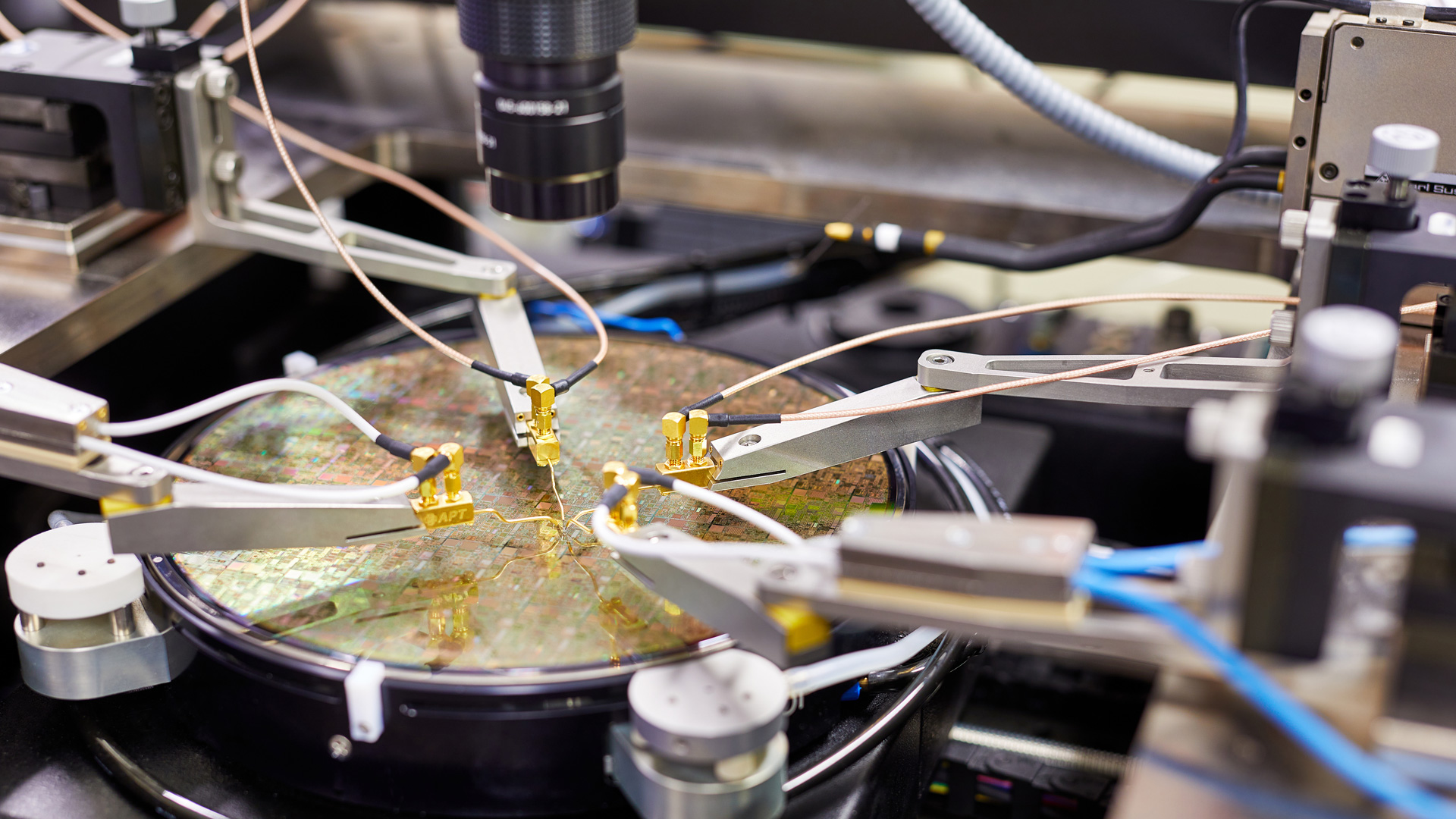
The continuous scaling and development of purely silicon-based microelectronic devices is gradually reaching its physical limits. Group III-V compound semiconductors have emerged as promising candidates to overcome these limitations due to their superior properties (e.g. in carrier mobility and ability to create band gaps). This makes III-V semiconductors interesting for use in electronic devices, as well as in active photonic components and in quantum technology. At the center of our research focus “III/V-on-Si” is the objective of co-integrating III-V materials on silicon to enable high-performance, low-cost systems that combine the advantageous III-V properties and functions with the mature mainstream silicon manufacturing technology. In this context, we are committed to researching III-V materials, processes and devices using our new FMD-funded exploratory process line in our clean room for future realization in a CMOS+X-compatible context.
Research Results
Script list Publications
C. Acal, D. Maldonado, A. Cantudo, M.B. González, F. Jiménez-Molinos, F. Campabadal, J.B. Roldán
Nanoscale 16(22), 10812 (2024)
DOI: 10.1039/D4NR01237B
A new statistical analysis is presented to assess cycle-to-cycle variability in resistive memories. This method employs two-dimensional (2D) distributions of parameters to analyse both set and reset voltages and currents, coupled with a 2D coefficient of variation (CV). This 2D methodology significantly enhances the analysis, providing a more thorough and comprehensive understanding of the data compared to conventional one-dimensional methods. Resistive switching (RS) data from two different technologies based on hafnium oxide are used in the variability study. The 2D CV allows a more compact assessment of technology suitability for applications such as non-volatile memories, neuromorphic computing and random number generation circuits.
(2) Electrically Pumped GeSn/SiGeSn Lasers
D. Buca, T. Liu, L. Seidel, O. Concepción, J.M. Hartmann, A. Tchelnokov, G. Capellini, M. Oehme, D. Grützmacher
ECS Meeting Abstracts MA2024-02, 2324 (2024)
DOI: 10.1149/MA2024-02322324mtgabs
(3) Low-Power Consumption IGZO Memristor-Based Gas Sensor Embedded in an Internet of Things Monitoring System for Isopropanol Alcohol Gas
M. Chae, D. Lee, H.-D. Kim
Micromachines (MDPI) 15(1), 77 (2024)
DOI: 10.3390/mi15010077
Low-power-consumption gas sensors are crucial for diverse applications, including environmental monitoring and portable Internet of Things (IoT) systems. However, the desorption and adsorption characteristics of conventional metal oxide-based gas sensors require supplementary equipment, such as heaters, which is not optimal for low-power IoT monitoring systems. Memristor-based sensors (gasistors) have been investigated as innovative gas sensors owing to their advantages, including high response, low power consumption, and room-temperature (RT) operation. Based on IGZO, the proposed isopropanol alcohol (IPA) gas sensor demonstrates a detection speed of 105 s and a high response of 55.15 for 50 ppm of IPA gas at RT. Moreover, rapid recovery to the initial state was achievable in 50 μs using pulsed voltage and without gas purging. Finally, a low-power circuit module was integrated for wireless signal transmission and processing to ensure IoT compatibility. The stability of sensing results from gasistors based on IGZO has been demonstrated, even when integrated into IoT systems. This enables energy-efficient gas analysis and real-time monitoring at ~0.34 mW, supporting recovery via pulse bias. This research offers practical insights into IoT gas detection, presenting a wireless sensing system for sensitive, low-powered sensors.
(4) Fast Circuit Simulation of Memristive Crossbar Arrays with Bimodal Stochastic Synaptic Weights
N. Dersch, C. Roemer, E. Perez, Ch. Wenger, M. Schwarz, B. Iniguez, A. Kloes
Proc. IEEE Latin American Electron Devices Conference (LAEDC 2024), (2024)
DOI: 10.1109/LAEDC61552.2024.10555829, (KI-IoT)
(5) A Flexible and Fast Digital Twin for RRAM Systems Applied for Training Resilient Neural Networks
M. Fritscher, S. Singh, T. Rizzi, A. Baroni, D. Reiser, M. Mallah, D. Hartmann, A. Bende, T. Kempen, M. Uhlmann, G. Kahmen, D. Fey, V. Rana, S. Menzel, M. Reichenbach, M. Krstic, F. Merchant, Ch. Wenger
Scientific Reports 14, 23695 (2024)
DOI: 10.1038/s41598-024-73439-z, (6G-RIC)
Resistive Random Access Memory (RRAM) has gained considerable momentum due to its non-volatility and energy efficiency. Material and device scientists have been proposing novel material stacks that can mimic the “ideal memristor” which can deliver performance, energy efficiency, reliability and accuracy. However, designing RRAM-based systems is challenging. Engineering a new material stack, designing a device, and experimenting takes significant time for material and device researchers. Furthermore, the acceptability of the device is ultimately decided at the system level. We see a gap here where there is a need for facilitating material and device researchers with a “push button” modeling framework that allows to evaluate the efficacy of the device at system level during early device design stages. Speed, accuracy, and adaptability are the fundamental requirements of this modelling framework. In this paper, we propose a digital twin (DT)-like modeling framework that automatically creates RRAM device models from device measurement data. Furthermore, the model incorporates the peripheral circuit to ensure accurate energy and performance evaluations. We demonstrate the DT generation and DT usage for multiple RRAM technologies and applications and illustrate the achieved performance of our GPU implementation. We conclude with the application of our modeling approach to measurement data from two distinct fabricated devices, validating its effectiveness in a neural network processing an Electrocardiogram (ECG) dataset and incorporating Fault Aware Training (FAT).
(6) From Device to Application - Integrating RRAM Accelerator Blocks into Large AI Systems
M. Fritscher, Ch. Wenger, M. Krstic
Proc. IEEE Computer Society Annual Symposium on VLSI (ISVLSI 2024), 592 (2024)
DOI: 10.1109/ISVLSI61997.2024.00111, (6G-RIC)
(7) From Device to Application - Integrating RRAM Accelerator Blocks into Large AI Systems
M. Fritscher, Ch. Wenger, M. Krstic
Proc. IEEE Computer Society Annual Symposium on VLSI (ISVLSI 2024), 592 (2024)
DOI: 10.1109/ISVLSI61997.2024.00111, (iCampus II)
(8) A Flexible and Fast Digital Twin for RRAM Systems Applied for Training Resilient Neural Networks
M. Fritscher, S. Singh, T. Rizzi, A. Baroni, D. Reiser, M. Mallah, D. Hartmann, A. Bende, T. Kempen, M. Uhlmann, G. Kahmen, D. Fey, V. Rana, S. Menzel, M. Reichenbach, M. Krstic, F. Merchant, Ch. Wenger
Scientific Reports 14, 23695 (2024)
DOI: 10.1038/s41598-024-73439-z, (iCampus II)
Resistive Random Access Memory (RRAM) has gained considerable momentum due to its non-volatility and energy efficiency. Material and device scientists have been proposing novel material stacks that can mimic the “ideal memristor” which can deliver performance, energy efficiency, reliability and accuracy. However, designing RRAM-based systems is challenging. Engineering a new material stack, designing a device, and experimenting takes significant time for material and device researchers. Furthermore, the acceptability of the device is ultimately decided at the system level. We see a gap here where there is a need for facilitating material and device researchers with a “push button” modeling framework that allows to evaluate the efficacy of the device at system level during early device design stages. Speed, accuracy, and adaptability are the fundamental requirements of this modelling framework. In this paper, we propose a digital twin (DT)-like modeling framework that automatically creates RRAM device models from device measurement data. Furthermore, the model incorporates the peripheral circuit to ensure accurate energy and performance evaluations. We demonstrate the DT generation and DT usage for multiple RRAM technologies and applications and illustrate the achieved performance of our GPU implementation. We conclude with the application of our modeling approach to measurement data from two distinct fabricated devices, validating its effectiveness in a neural network processing an Electrocardiogram (ECG) dataset and incorporating Fault Aware Training (FAT).
(9) Area-Efficient Digital Design using RRAM-CMOS Standardcells
M. Fritscher, M. Uhlmann, P. Ostrovskyy, D. Reiser, J.-C. Chen, M.A. Schubert, C. Schulze, G. Kahmen, D. Fey, M. Reichenbach, M. Kristic, Ch. Wenger
Proc. IEEE Computer Society Annual Symposium on VLSI (ISVLSI 2024), 81 (2024)
DOI: 10.1109/ISVLSI61997.2024.00026, (iCampus II)
(10) Area-Efficient Digital Design using RRAM-CMOS Standardcells
M. Fritscher, M. Uhlmann, P. Ostrovskyy, D. Reiser, J.-C. Chen, M.A. Schubert, C. Schulze, G. Kahmen, D. Fey, M. Reichenbach, M. Kristic, Ch. Wenger
Proc. IEEE Computer Society Annual Symposium on VLSI (ISVLSI 2024), 81 (2024)
DOI: 10.1109/ISVLSI61997.2024.00026, (HYB-RISC)
(11) Area-Efficient Digital Design using RRAM-CMOS Standardcells
M. Fritscher, M. Uhlmann, P. Ostrovskyy, D. Reiser, J.-C. Chen, M.A. Schubert, C. Schulze, G. Kahmen, D. Fey, M. Reichenbach, M. Kristic, Ch. Wenger
Proc. IEEE Computer Society Annual Symposium on VLSI (ISVLSI 2024), 81 (2024)
DOI: 10.1109/ISVLSI61997.2024.00026, (KI-IoT)
(12) A Flexible and Fast Digital Twin for RRAM Systems Applied for Training Resilient Neural Networks
M. Fritscher, S. Singh, T. Rizzi, A. Baroni, D. Reiser, M. Mallah, D. Hartmann, A. Bende, T. Kempen, M. Uhlmann, G. Kahmen, D. Fey, V. Rana, S. Menzel, M. Reichenbach, M. Krstic, F. Merchant, Ch. Wenger
Scientific Reports 14, 23695 (2024)
DOI: 10.1038/s41598-024-73439-z, (MIMEC)
Resistive Random Access Memory (RRAM) has gained considerable momentum due to its non-volatility and energy efficiency. Material and device scientists have been proposing novel material stacks that can mimic the “ideal memristor” which can deliver performance, energy efficiency, reliability and accuracy. However, designing RRAM-based systems is challenging. Engineering a new material stack, designing a device, and experimenting takes significant time for material and device researchers. Furthermore, the acceptability of the device is ultimately decided at the system level. We see a gap here where there is a need for facilitating material and device researchers with a “push button” modeling framework that allows to evaluate the efficacy of the device at system level during early device design stages. Speed, accuracy, and adaptability are the fundamental requirements of this modelling framework. In this paper, we propose a digital twin (DT)-like modeling framework that automatically creates RRAM device models from device measurement data. Furthermore, the model incorporates the peripheral circuit to ensure accurate energy and performance evaluations. We demonstrate the DT generation and DT usage for multiple RRAM technologies and applications and illustrate the achieved performance of our GPU implementation. We conclude with the application of our modeling approach to measurement data from two distinct fabricated devices, validating its effectiveness in a neural network processing an Electrocardiogram (ECG) dataset and incorporating Fault Aware Training (FAT).
(13) Characterization of Drop Cast as Strategy for the Biofunctionalization of Plasmonic Sensors Based on Highly Doped Ge-Based
E. Hardt, R. Varricchio, C.A. Chavarin, O. Skibitzki, A. di Masi, G. Capellini
Proc. iCampus Cottbus Conference (iCCC 2024), 191 (2024)
DOI: 10.5162/iCCC2024/P24, (iCampus II)
(14) Investigation of Defect Formation in Monolithic Integrated GaP Islands on Si Nanotips Wafers
I. Häusler, R. Repa, A. Hammud, O. Skibitzki, F. Hatami
Electronics (MDPI) 13(15), 2945 (2024)
DOI: 10.3390/electronics13152945, (NHEQuanLEA)
The monolithic integration of gallium phosphide (GaP), with its green band gap, high refractive index, large optical non-linearity, and broad transmission range on silicon (Si) substrates, is crucial for Si-based optoelectronics and integrated photonics. However, material mismatches, including thermal expansion mismatch and polar/non-polar interfaces, cause defects such as stacking faults, microtwins, and anti-phase domains in GaP, adversely affecting its electronic properties. Our paper presents a structural and defect analysis using scanning transmission electron microscopy, high-resolution transmission electron microscopy, and scanning nanobeam electron diffraction of epitaxial GaP islands grown on Si nanotips embedded in SiO2. The Si nanotips were fabricated on 200 mm n-type Si (001) wafers using a CMOS-compatible pilot line, and GaP islands were grown selectively on the tips via gas-source molecular-beam epitaxy. Two sets of samples were investigated: GaP islands nucleated on open Si nanotips and islands nucleated within self-organized nanocavities on top of the nanotips. Our results reveal that in both cases, the GaP islands align with the Si lattice without dislocations due to lattice mismatch. Defects in GaP islands are limited to microtwins and stacking faults. When GaP nucleates in the nanocavities, most defects are trapped, resulting in defect-free GaP islands. Our findings demonstrate an effective approach to mitigate defects in epitaxial GaP on Si nanotip wafers fabricated by CMOS-compatible processes.
(15) Structural and Morphological Properties of CeO2 Films Deposited by Radio Frequency Magnetron Sputtering for Back-End-of-Line Integration
A. Hayat, M. Ratzke, C.A. Chavarin, M.H. Zoellner, A.A. Corley-Wiciak, M.A. Schubert, Ch. Wenger, I.A. Fischer
Thin Solid Films 807, 140547 (2024)
DOI: 10.1016/j.tsf.2024.140547, (iCampus II)
Cerium oxides have potential applications ranging from low-temperature gas sensing to photodetection. A back-end-of-line integration of the material into complementary metal-oxide-semiconductor device fabrication processes has many advantages but places limits on material deposition, most notably the thermal budget for deposition and annealing. Here, we investigate thin cerium oxide films deposited by radio frequency (RF) magnetron sputtering at substrate temperatures of 300°C and RF magnetron powers between 30 W and 70 W without any post-deposition annealing steps. Our investigation of the structural and morphological properties reveals a columnar texture of the thin films, and we find that the material is composed predominantly of CeO2 (111), with a large degree of crystallinity. We discuss implications for resistive gas sensing applications.
(16) Soft-Error Analysis of RRAM 1T1R Compute-In-Memory Core for Artificial Neural Networks
R Jia, S. Pechmann, M. Fritscher, Ch. Wenger, L. Zhang, A. Hagelauer
Proc. 39th Conference on Design of Circuits and Integrated Systems (DCIS 2024), (2024)
DOI: 10.1109/DCIS62603.2024.10769203, (MIMEC)
(17) Selective Growth of GaP Crystals on CMOS-Compatible Si Nanotip Wafers by Gas Source Molecular Beam Epitaxy
N. Kafi, S. Kang, C. Golz, A. Rodrigues-Weisensee, L. Persichetti, D. Ryzhak, G. Capellini, D. Spirito, M. Schmidbauer, A. Kwasniewski, C. Netzel, O. Skibitzki, F. Hatami
Crystal Growth & Design 24(7), 2724 (2024)
DOI: 10.1021/acs.cgd.3c01337, (NHEQuanLEA)
Gallium phosphide (GaP) is a III–V semiconductor with remarkable optoelectronic properties, and it has almost the same lattice constant as silicon (Si). However, to date, the monolithic and large-scale integration of GaP devices with silicon remains challenging. In this study, we present a nanoheteroepitaxy approach using gas-source molecular-beam epitaxy for selective growth of GaP islands on Si nanotips, which were fabricated using complementary metal–oxide semiconductor (CMOS) technology on a 200 mm n-type Si(001) wafer. Our results show that GaP islands with sizes on the order of hundreds of nanometers can be successfully grown on CMOS-compatible wafers. These islands exhibit a zinc-blende phase and possess optoelectronic properties similar to those of a high-quality epitaxial GaP layer. This result marks a notable advancement in the seamless integration of GaP-based devices with high scalability into Si nanotechnology and integrated optoelectronics.
(18) Controlled Integration of InP Nanoislands with CMOS-Compatible Si using Nanoheteroepitaxy Approach
A. Kamath, D. Ryzhak, A. Rodrigues, N. Kafi, C. Golz, D. Spirito, O. Skibitzki, L. Persichetti, M. Schmidbauer, F. Hatami
Materials Science in Semiconductor Processing 182, 108585 (2024)
DOI: 10.1016/j.mssp.2024.108585, (NHEQuanLEA)
Indium phosphide (InP) nanoislands are grown on pre-patterned Silicon (001) nanotip substrate using gas-source molecular-beam epitaxy via nanoheteroepitaxy approach. The study explores the critical role of growth temperature in achieving selectivity, governed by diffusion length. Our study reveals that temperatures of about 480 °C and lower, lead to parasitic growth, while temperatures about 540 °C with an indium growth rate of about 0.7 Å.s−1 and phosphine flux of 4 sccm inhibit selective growth. The establishment of an optimal temperature window for selective InP growth is demonstrated for a temperature range of 490 °C to 530 °C. Comprehensive structural and optical analyses using atomic force microscopy, Raman spectroscopy, x-ray diffraction, and photoluminescence confirm a zincblende structure of indium phosphide with fully relaxed islands. These results demonstrate the capability to precisely tailor the position of InP nanoislands through a noncatalytic nanoheteroepitaxy approach, marking a crucial advancement in integrating InP nanoisland arrays on silicon devices.
(19) Comparison of a Binary Signed-Digit Adder with Conventional Binary Adder Circuits on Layout Level
J. Kliemt, M. Fritscher, D. Fey
Proc. 37th GI/ITG International Conference on Architecture of Computing Systems (ARCS 2024), in: Lecture Notes in Computer Science, Springer, LNCS 14842, 236 (2024)
(HYB-RISC)
(20) Rational Design and Development of Room Temperature Hydrogen Sensors Compatible with CMOS Technology: A Necessary Step for the Coming Renewable Hydrogen Economy
J. Kosto, R. Tschammer, C. Morales, K. Henkel, C.A. Chavarin, I. Costina, M. Ratzke, Ch. Wenger, I.A. Fischer, J.I. Flege
Proc. iCampus Conference Cottbus (iCCC 2024), 182 (2024)
DOI: 10.5162/iCCC2024/P21
(21) Kinetic Monte Carlo Simulation Analysis of the Conductance Drift in Multilevel HfO2-based RRAM Devices
D. Maldonado, A. Baroni, S. Aldana, K.D.S. Reddy, S. Pechmann, Ch. Wenger, J.B. Roldán, E. Pérez
Nanoscale 16(40), 19021 (2024)
DOI: 10.1039/d4nr02975e, (KI-IoT)
This study investigates the retention and drift characteristics of valence change memory (VCM) devices through both experimental analysis and a 3D kinetic Monte Carlo (kMC) simulation approach. By simulating six distinct low-resistance states (LRS) over a 24-hour period at room temperature, we aim to assess the temporal stability and endurance of these devices. Our results demonstrate the feasibility of multi-level operation and reveal insights into conductive filament (CF) dynamics, including percolation path analysis and oxygen vacancy behavior. The cumulative distribution functions (CDFs) of read-out currents measured at different time intervals provide a comprehensive view of the performance of the devices across different LRS. These findings not only enhance the understanding of VCM device behavior but also inform strategies for improving retention and mitigating drift, thereby advancing the development of reliable nonvolatile resistive switching memory technologies.
(22) Influence of Stop and Gate Voltage on Resistive Switching of 1T1R HfO2-based Memristors, a Modeling and Variability Analysis
D. Maldonado, A. Cantudo, K.D.S. Reddy, S. Pechmann, M. Uhlmann, Ch. Wenger, J.B. Roldán, E. Pérez
Materials Science in Semiconductor Processing 182, 108726 (2024)
DOI: 10.1016/j.mssp.2024.108726, (KI-IoT)
Memristive devices, particularly resistive random access memory (RRAM) cells based on hafnium oxide (HfO₂) dielectrics, exhibit promising characteristics for a wide range of applications. In spite of their potential, issues related to intrinsic variability and the need for precise simulation tools and modeling methods remain a medium-term hurdle. This study addresses these challenges by investigating the resistive switching (RS) behavior of different 1T1R HfO₂-based memristors under various experimental conditions. Through a comprehensive experimental analysis, we extract RS parameters using different numerical techniques to understand the cycle-to-cycle (C2C) and device-to-device (D2D) variability. Additionally, we employ advanced simulation methodologies, including circuit breaker-based 3D simulation, to shed light on our experimental findings and provide a theoretical framework to disentangle the switching phenomena. Our results offer valuable insights into the RS mechanisms and variability, contributing to the improvement of robust parameter extraction methods, which are essential for the industrial application of memristive devices.
(23) The Effects of Substrate Interaction on the Chemical Properties of Atomic Layer Deposited Ultrathin Ceria Layers
C. Morales, R. Tschammer, J. Kosto, C.A. Chavarin, Ch. Wenger, I. Villar-Garcia, V. Pérez-Dieste, K. Henkel, J.I. Flege
Proc. European Conference on Applications of Surface and Interface Analysis (ECASIA 2024), abstr. book (2024)
(iCampus II)
(24) Blooming and Pruning: Learning from Mistakes with Memristive Synapses
K. Nikiruy, E. Perez, A. Baroni, K.D.S. Reddy, S. Pechmann, Ch. Wenger, M. Ziegler
Scientific Reports 14, 7802 (2024)
DOI: 10.1038/s41598-024-57660-4, (KI-IoT)
Blooming and pruning is one of the most important developmental mechanisms of the biological brain in the first years of life, enabling it to adapt its network structure to the demands of the environment. The mechanism is thought to be fundamental for the development of cognitive skills. Inspired by this, Chialvo and Bak proposed in 1999 a learning scheme that learns from mistakes by eliminating from the initial surplus of synaptic connections those that lead to an undesirable outcome. Here, this idea is implemented in a neuromorphic circuit scheme using CMOS integrated HfO2-based memristive devices. The implemented two-layer neural network learns in a self-organized manner without positive reinforcement and exploits the inherent variability of the memristive devices. A combined experimental and simulation-based parameter study is presented to find the relevant system and device parameters leading to a compact and robust memristive neuromorphic circuit that can handle association tasks.
(25) A Current Mirror Based Read Circuit Design with Multi-Level Capability for Resistive Switching Devices
S. Pechmann, E. Perez, Ch. Wenger, A. Hagelauer
Proc. International Conference on Electronics, Information, and Communication (ICEIC 2024), (2024)
DOI: 10.1109/ICEIC61013.2024.10457188, (KI-IoT)
(26) Forming and Resistive Switching of HfO2-Based RRAM Devices at Cryogenic Temperature
E. Perez-Bosch Quesada, A. Mistroni, R. Jia, K.D.S. Reddy, F. Reichmann, Ch. Wenger, E. Perez
IEEE Electron Device Letters 45(12), 2391 (2024)
DOI: 10.1109/LED.2024.3485873, (KI-PRO)
Reliable data storage technologies able to operate at cryogenic temperatures are critical to implement scalable quantum computers and develop deep-space exploration systems, among other applications. Their scarce availability is pushing towards the development of emerging memories that can perform such storage in a non-volatile fashion. Resistive Random-Access Memories (RRAM) have demonstrated their switching capabilities down to 4 K. However, their operability at lower temperatures still remain as a challenge. In this work, we demonstrate for the first time the forming and resistive switching capabilities of CMOS-compatible RRAM devices at 1.4 K. The HfO2 -based devices are deployed following an array of 1-transistor-1-resistor (1T1R) cells. Their switching performance at 1.4K was also tested in the multilevel-cell (MLC) approach, storing up to 4 resistance levels per cell.
(27) Forming and Resistive Switching of HfO2-Based RRAM Devices at Cryogenic Temperature
E. Perez-Bosch Quesada, A. Mistroni, R. Jia, K.D.S. Reddy, F. Reichmann, Ch. Wenger, E. Perez
IEEE Electron Device Letters 45(12), 2391 (2024)
DOI: 10.1109/LED.2024.3485873, (MIMEC)
Reliable data storage technologies able to operate at cryogenic temperatures are critical to implement scalable quantum computers and develop deep-space exploration systems, among other applications. Their scarce availability is pushing towards the development of emerging memories that can perform such storage in a non-volatile fashion. Resistive Random-Access Memories (RRAM) have demonstrated their switching capabilities down to 4 K. However, their operability at lower temperatures still remain as a challenge. In this work, we demonstrate for the first time the forming and resistive switching capabilities of CMOS-compatible RRAM devices at 1.4 K. The HfO2 -based devices are deployed following an array of 1-transistor-1-resistor (1T1R) cells. Their switching performance at 1.4K was also tested in the multilevel-cell (MLC) approach, storing up to 4 resistance levels per cell.
(28) Forming and Resistive Switching of HfO2-Based RRAM Devices at Cryogenic Temperature
E. Perez-Bosch Quesada, A. Mistroni, R. Jia, K.D.S. Reddy, F. Reichmann, Ch. Wenger, E. Perez
IEEE Electron Device Letters 45(12), 2391 (2024)
DOI: 10.1109/LED.2024.3485873, (KI-IoT)
Reliable data storage technologies able to operate at cryogenic temperatures are critical to implement scalable quantum computers and develop deep-space exploration systems, among other applications. Their scarce availability is pushing towards the development of emerging memories that can perform such storage in a non-volatile fashion. Resistive Random-Access Memories (RRAM) have demonstrated their switching capabilities down to 4 K. However, their operability at lower temperatures still remain as a challenge. In this work, we demonstrate for the first time the forming and resistive switching capabilities of CMOS-compatible RRAM devices at 1.4 K. The HfO2 -based devices are deployed following an array of 1-transistor-1-resistor (1T1R) cells. Their switching performance at 1.4K was also tested in the multilevel-cell (MLC) approach, storing up to 4 resistance levels per cell.
(29) Thermal Compact Modeling and Resistive Switching Analysis in Titanium Oxide-Based Memristors
J.B. Roldán, A. Cantudo, D. Maldonado, C. Aguilera-Pedregosa, E. Moreno, T. Swoboda, F. Jimenez-Molinos, Y. Yuan, K. Zhu, M. Lanza, M.M. Rojo
ACS Applied Electronic Materials 6(2), 1424 (2024)
DOI: 10.1021/acsaelm.3c01727, (KI-IoT)
Resistive switching devices based on the Au/Ti/TiO2/Au stack were developed. In addition to standard electrical characterization by means of I–V curves, scanning thermal microscopy was employed to localize the hot spots on the top device surface (linked to conductive nanofilaments, CNFs) and perform in-operando tracking of temperature in such spots. In this way, electrical and thermal responses can be simultaneously recorded and related to each other. In a complementary way, a model for device simulation (based on COMSOL Multiphysics) was implemented in order to link the measured temperature to simulated device temperature maps. The data obtained were employed to calculate the thermal resistance to be used in compact models, such as the Stanford model, for circuit simulation. The thermal resistance extraction technique presented in this work is based on electrical and thermal measurements instead of being indirectly supported by a single fitting of the electrical response (using just I–V curves), as usual. Besides, the set and reset voltages were calculated from the complete I–V curve resistive switching series through different automatic numerical methods to assess the device variability. The series resistance was also obtained from experimental measurements, whose value is also incorporated into a compact model enhanced version.
(30) Stochastic Resonance in 2D Materials Based Memristors
J.B. Roldán, A. Cantudo, J.J. Torres, D. Maldonado, Y. Shen, W. Zheng, Y. Yuan, M. Lanza
npj 2D Materials and Applications 8, 7 (2024)
DOI: 10.1038/s41699-024-00444-1, (KI-IoT)
Stochastic resonance is an essential phenomenon in neurobiology, it is connected to the constructive role of noise in the signals that take place in neuronal tissues, facilitating information communication, memory, etc. Memristive devices are known to be the cornerstone of hardware neuromorphic applications since they correctly mimic biological synapses in many different facets, such as short/long-term plasticity, spike-timing-dependent plasticity, pair-pulse facilitation, etc. Different types of neural networks can be built with circuit architectures based on memristive devices (mostly spiking neural networks and artificial neural networks). In this context, stochastic resonance is a critical issue to analyze in the memristive devices that will allow the fabrication of neuromorphic circuits. We do so here with h-BN based memristive devices from different perspectives. It is found that the devices we have fabricated and measured clearly show stochastic resonance behaviour. Consequently, neuromorphic applications can be developed to account for this effect, that describes a key issue in neurobiology with strong computational implications.
(31) Nanoheteroepitaxy of Ge and SiGe on Si: Role of Composition and Capping on Quantum Dot Photoluminescence
D. Ryzhak, J. Aberl, E. Prado-Navarrete, L. Vukusic, A.A. Corley-Wiciak, O. Skibitzki, M.H. Zoellner, M.A. Schubert, M. Virgilio, M. Brehm, G. Capellini, D. Spirito
Nanotechnology 35(50), 505001 (2024)
DOI: 10.1088/1361-6528/ad7f5f, (NHEQuanLEA)
We investigate the nanoheteroepitaxy of SiGe and Ge quantum dots (QDs) grown on nanotips substrates realized in Si(001) wafers. Due to the lattice strain compliance, enabled by the nanometric size of the tip and the limited dot/substrate interface area, which helps to reduce dot/substrate interdiffusion, the strain and SiGe composition in the QDs could be decoupled. This demonstrates a key advantage of the nanoheteroepitaxy over the Stranski-Krastanow growth mechanism. Nearly semi-spherical, defect-free, ∼100 nm wide SiGe QDs with different Ge contents were successfully grown on the nanotips with high selectivity and size uniformity. On the dots, thin dielectric capping layers were deposited, improving the optical properties by the passivation of surface states. Intense photoluminescence was measured from all samples investigated with emission energy, intensity, and spectral linewidth dependent on the SiGe composition of the QDs and the different capping layers. Radiative recombination occurs in the QDs, and its energy matches the results of band-structure calculations that consider strain compliance between the QD and the tip. The nanotips arrangement and the selective growth of QDs allow to studying the PL emission from only 3-4 QDs, demonstrating a bright emission and the possibility of selective addressing. These findings will support the design of optoelectronic devices based on CMOS-compatible emitters.
(32) Selective Epitaxy of Germanium on Silicon for the Fabrication of CMOS Compatible Short-Wavelength Infrared Photodetectors
D. Ryzhak, A.A. Corley-Wiciak, P. Steglich, Y. Yamamoto, J. Frigerio, R. Giani, A. De Iacovo, D. Spirito, G. Capellini
Materials Science in Semiconductor Processing 176, 108308 (2024)
DOI: 10.1016/j.mssp.2024.108308, (VISIR2)
Here we present the selective epitaxial growth of Ge on Si using reduced pressure chemical vapor deposition on SiO2/Si solid masks realized on 200 mm Si wafers, aiming at manufacturing integrated visible/short-wavelength infrared photodetectors. By a suitable choice of the reactants and of the process conditions, we demonstrated highly selective and pattern-independent growth of Ge microstructure featuring high crystalline quality. The Ge “patches” show a distinct faceting, with a flat top (001) facet and low energy facets such as e.g. {113} and {103} at their sidewalls, independently on their size. Interdiffusion of Si in to the Ge microcrystals is limited to an extension of ∼20 nm from the heterointerface. The Ge patches resulted to be plastically relaxed with threading dislocation density values better or on par than those observed in continuous two-dimensional Ge/Si epilayer in the low 107 cm−2 range. A residual tensile strain was observed for patches with size >10 μm, due to elastic thermal strain accumulation, as confirmed by μ-Raman spectroscopy and μ-photoluminescence characterization. Polarization-dependent Raman mapping highlights the strain distribution associated to the tridimensional shape. On this material, Ge photodiodes were fabricated and characterized, showing promising optoelectronic performances.
(33) On the Asymmetry of Resistive Switching Transitions
G. Vinuesa, H. Garcia, E. Perez, Ch. Wenger, I. Iniguez-de-la-Torre, T. Gonzalez, S. Duenas, H. Castan
Electronics (MDPI) 13(13), 2639 (2024)
DOI: 10.3390/electronics13132639, (KI-IoT)
In this study, the resistive switching phenomena in TiN/Ti/HfO2/Ti metal–insulator–metal stacks is investigated, mainly focusing on the analysis of set and reset transitions. The electrical measurements in a wide temperature range reveal that the switching transitions require less voltage (and thus, less energy) as temperature rises, with the reset process being much more temperature sensitive. The main conduction mechanism in both resistance states is Space-charge-limited Conduction, but the high conductivity state also shows Schottky emission, explaining its temperature dependence. Moreover, the temporal evolution of these transitions reveals clear differences between them, as their current transient response is completely different. While the set is sudden, the reset process development is clearly non-linear, closely resembling a sigmoid function. This asymmetry between switching processes is of extreme importance in the manipulation and control of the multi-level characteristics and has clear implications in the possible applications of resistive switching devices in neuromorphic computing.