

Technologies for smart systems are an important foundation for IHP’s strategic research areas: technologies for Wireless & Broadband Communication, Sensors, Health & Environment, and technologies for Resilient Systems. To support these areas, the Technology department develops silicon- and germanium-based devices, modules, and technology platforms for communications, RF electronics, sensors, artificial intelligence, and quantum technologies.
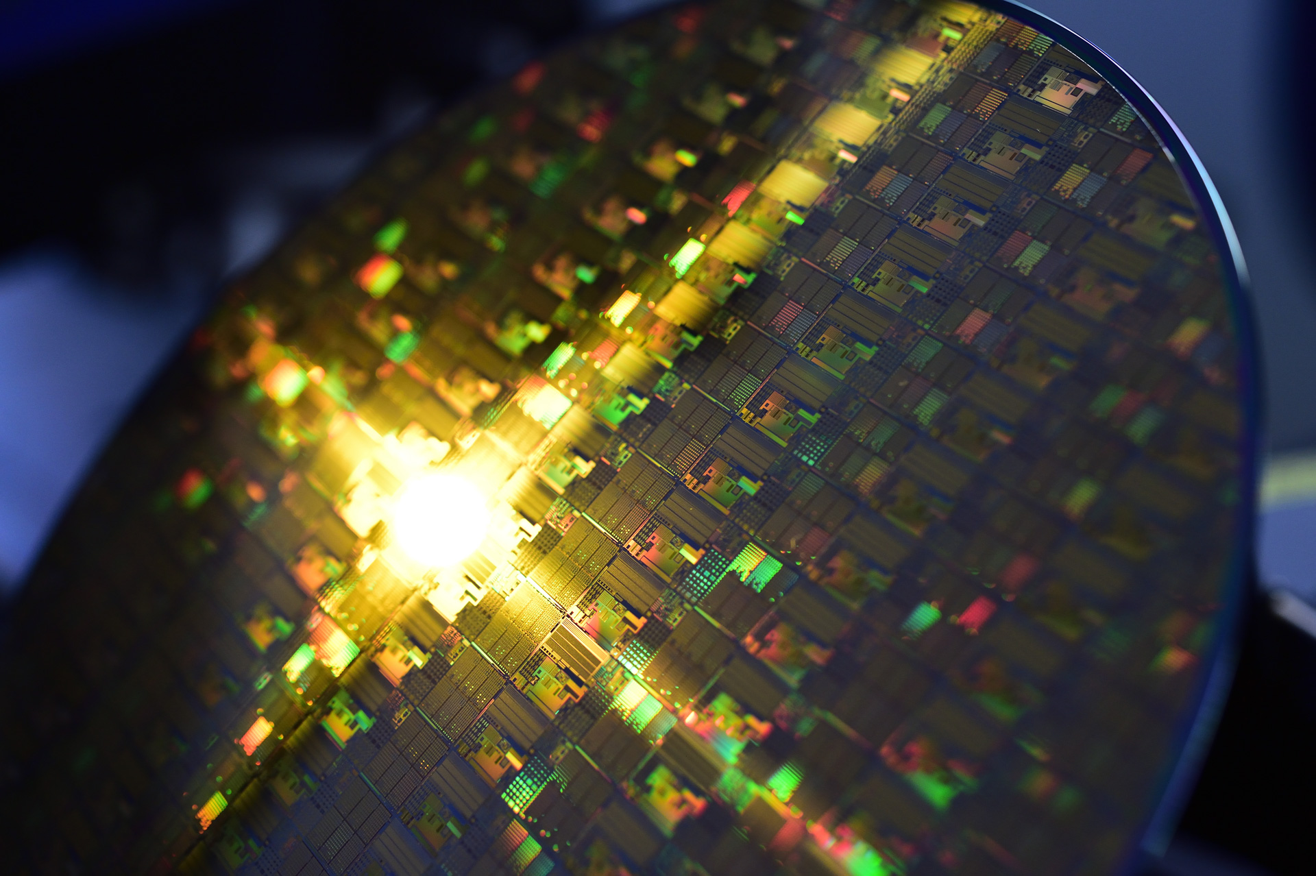
The focus is on the functional enhancement of CMOS technologies. To this end, the department develops and optimizes high-performance SiGe BiCMOS and photonics technologies based on IHP’s 200 mm silicon platform.
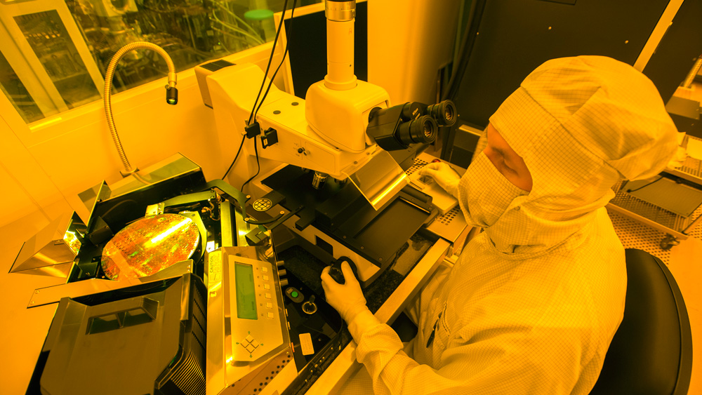
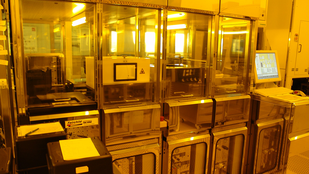
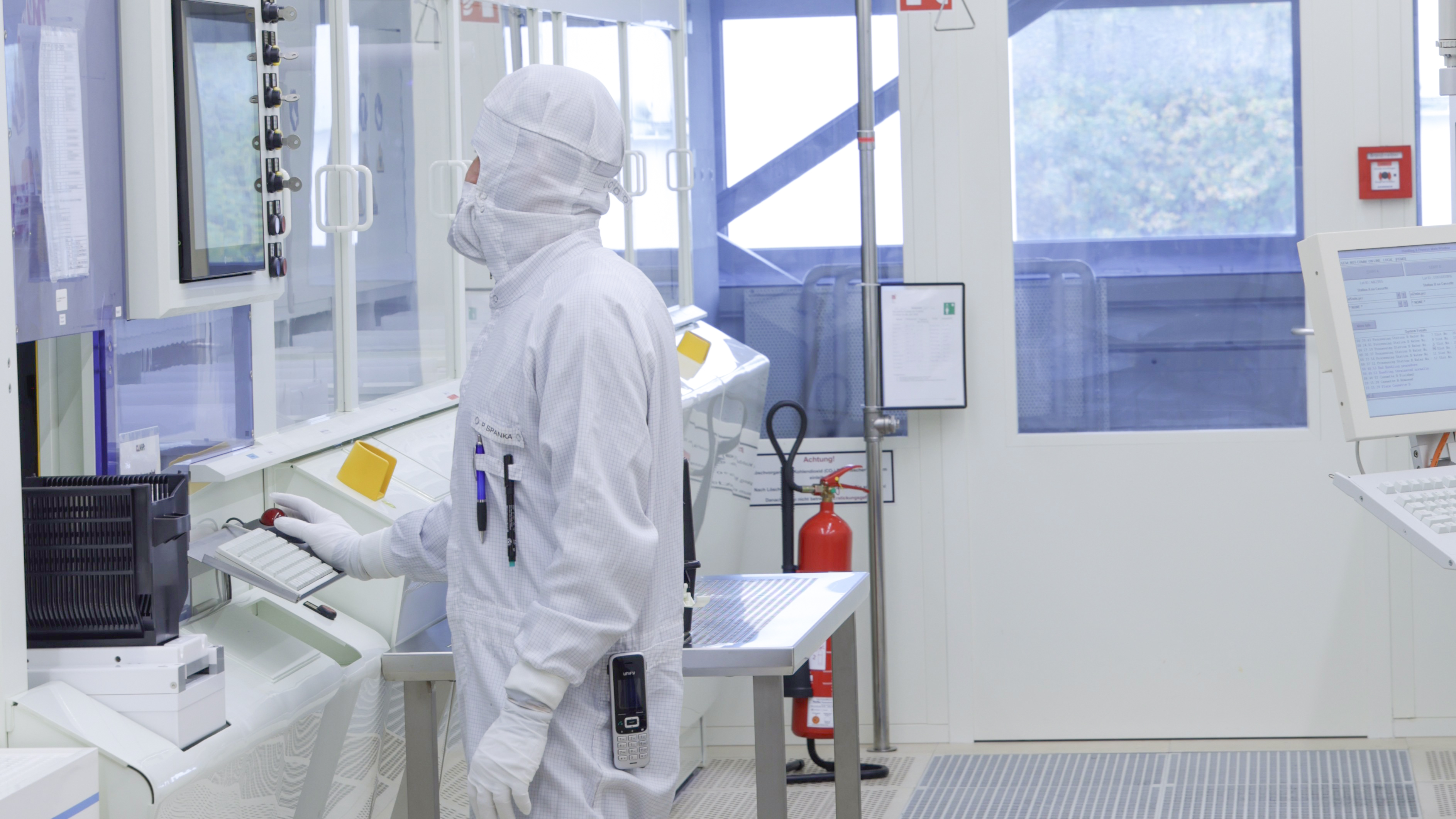
For more than 20 years, this technological expertise has provided the foundation for the department’s continuous development. Around half of IHP’s employees work in the department, including the staff who operate the cleanroom in continuous shifts.
A particular strength is the close integration of research, manufacturing, and services. New technologies are stabilized, quickly transferred to the IHP pilot line as technology platforms, and made available to partners through IHP’s research services for research and prototype manufacturing. The portfolio includes the Multi-Project Wafer (MPW) program as well as module and individual process-step development for 200 mm processes.
As part of Research Fab Microelectronics Germany, the department works with research partners on new process capabilities and technology developments. This expands both the research infrastructure and the available technology portfolio.
Capabilities
Development of SiGe BiCMOS and Photonics Technologies
The department develops and expands high-performance SiGe BiCMOS and photonics technologies based on IHP’s 200 mm silicon platform. This work includes new devices, process modules, and technology platforms that are compatible with silicon-based manufacturing, as well as modular extensions of standard CMOS technologies.
Technology Optimization and Qualification
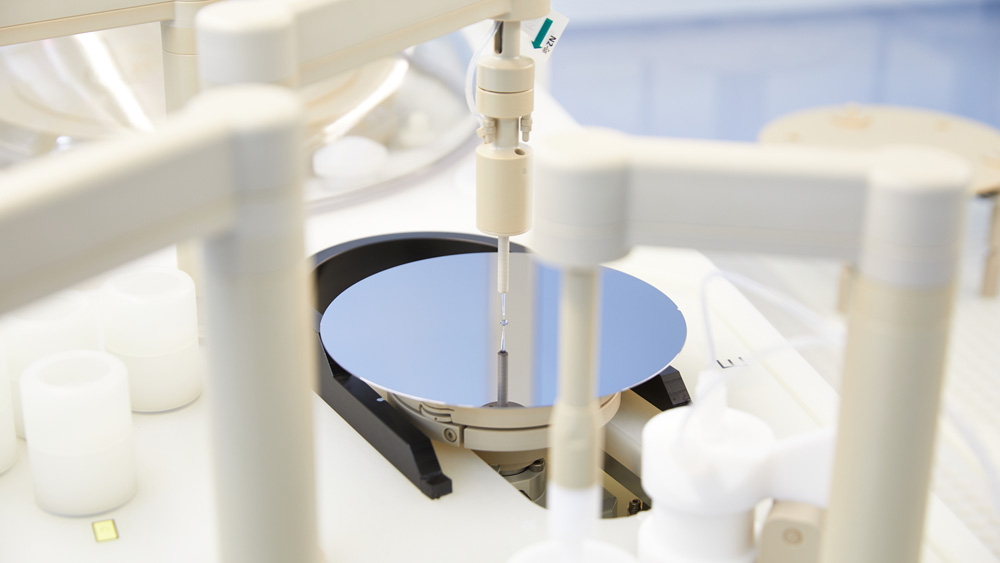
Existing IHP technologies are transferred, optimized, stabilized, and further developed to improve their performance. This work includes process qualification, reliability assessment, and the transfer of research results into stable processes for the cleanroom, which operates in a 24/7 mode.
THz and RF Technologies
Research includes SiGe-based THz devices and new integration concepts for RF systems. These technologies support applications in wireless and broadband communications using silicon-based electrical and optoelectronic RF components.
Silicon Photonics and Optoelectronics
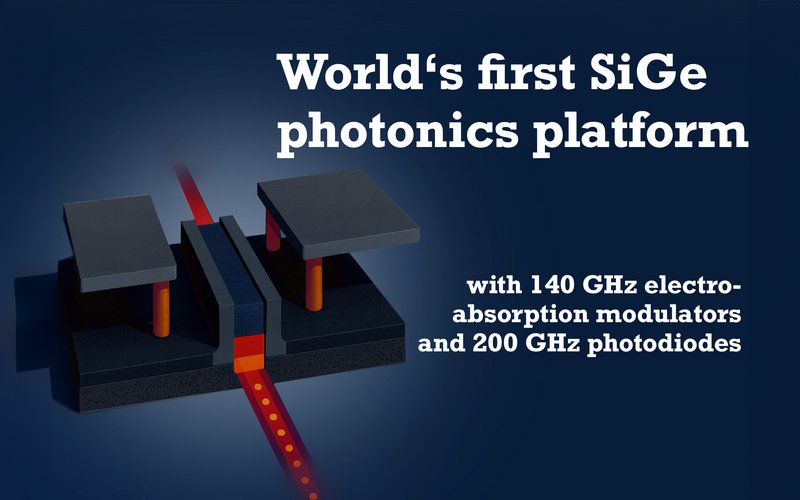
Activities in this area include the development of silicon-germanium photonics modules, including germanium photodetectors and modulators, and their integration into BiCMOS technologies. Research also focuses on complex silicon photonics platforms and photonic sensors for health and environmental analysis.
Novel Materials and Devices
New materials and devices are integrated into silicon-based technologies. These include memristive cells for artificial intelligence applications as well as devices for radiation-resistant systems.
Monolithic and Heterogeneous Integration
Advanced and multi-technology integration concepts are the objective of this research which includes approaches to (quasi)-monolithic and heterogeneous integration in which electronics and additional module functions are combined on a single chip or within an integrated system. The methods used include wafer bonding and chip transfer for the heterogeneous integration of chiplets.
Process and Device Characterization
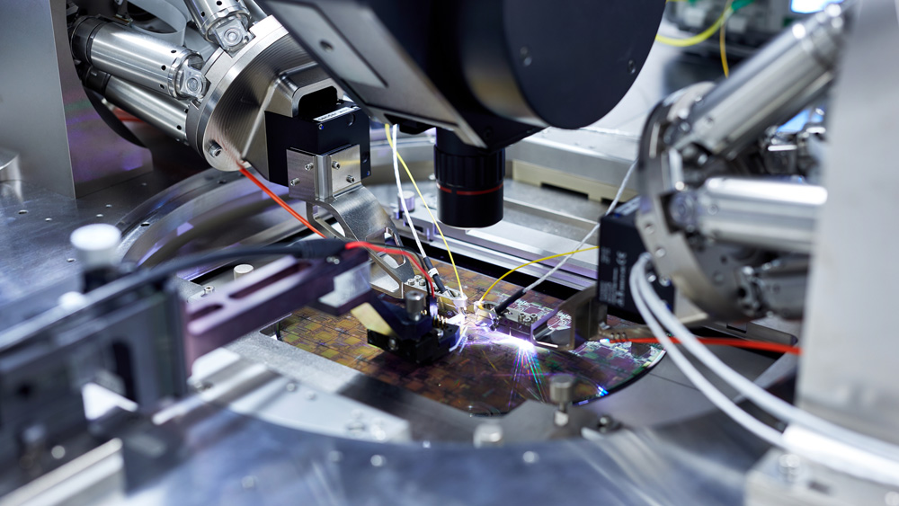
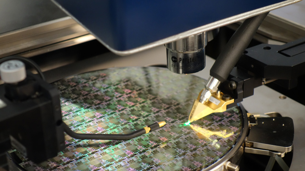
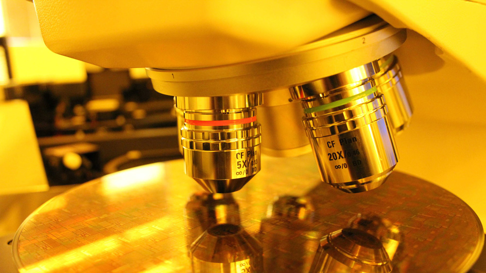
Capabilities include electrical and optoelectronic measurements, RF testing, materials analysis, process diagnostics, device modeling, functional testing, and reliability assessments.
Services
IHP has all the capabilities required to develop and manufacture state-of-the-art SiGe BiCMOS technologies. The department offers research, module, MPW, and prototyping services to scientific and industrial partners worldwide. These include:
- Access to 0.13 µm technologies through MPW and prototyping programs
- Research and prototype manufacturing using newly developed technologies
- Development of process modules and individual process steps for 200 mm technologies
- Integration of SiGe and photonics modules into CMOS technologies
- Modular extension of standard CMOS technologies
- Integration of new materials into silicon-based processes
- Electrical, optoelectronic, and RF characterization
- Diagnostic analyses, reliability testing, and process qualification
- Design kit support for internal and external projects
- Transfer of technologies and technology modules to and from industrial partners
- Stabilization and transfer of research technologies into IHP’s research and manufacturing services