SiGe BiCMOS and Silicon Photonics Technologies
IHP offers standard 0.13 and 0.25 μm CMOS processes which provide NMOS, PMOS, isolated NMOS and passive components such as poly resistors and MIM capacitors. In addition to the standard CMOS processes different front-end-of-line options are offered. In 0.25 μm CMOS the standard backend offers 3 thin metal layers and two TopMetal layers (TopMetal1 - fourth 2 μm thick metal layer, TopMetal2 – fifth 3 μm thick metal layer). The backend for 0.13 μm process offers 5 thin and 2 thick metal layers (TM1: 2 μm TM2: 3 μm). Together with a high dielectric stack this enables increased performance of the passive RF components.
Technologies with an enhanced BEOL option with copper are offered.
A commercial MPW service is offered through IHP Solutions.
Please click for: MPW Schedule and Price Information
Technologies for MPW & Prototyping
Detailed specifications for all the IHP technologies can be found here.
SG13S is a high-performance 0.13 μm BiCMOS technology with npn-HBTs with cutoff frequencies up to fT= 250 GHz and fmax = 340 GHz, with 3.3 V I/O CMOS and 1.2 V logic CMOS.
SG13G2 is a 0.13 μm BiCMOS technology with same device portfolio as SG13S, but significantly higher bipolar performance with fT/fmax = 350/450 GHz.
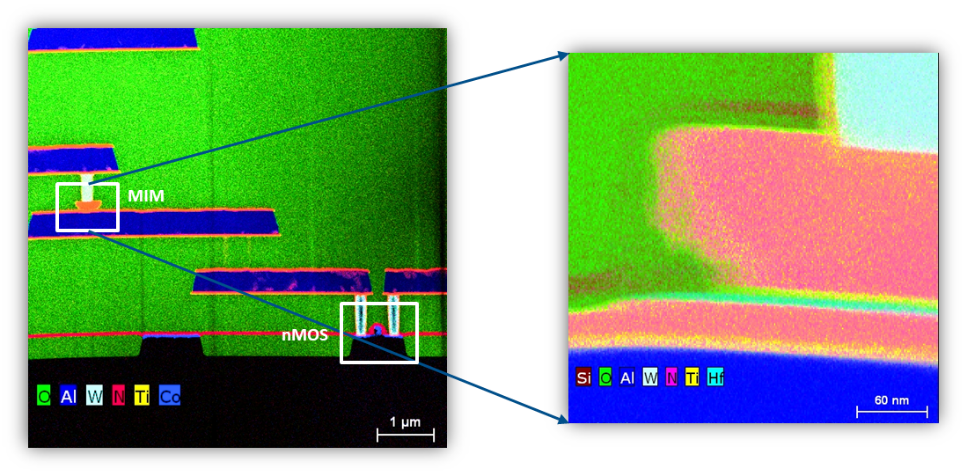
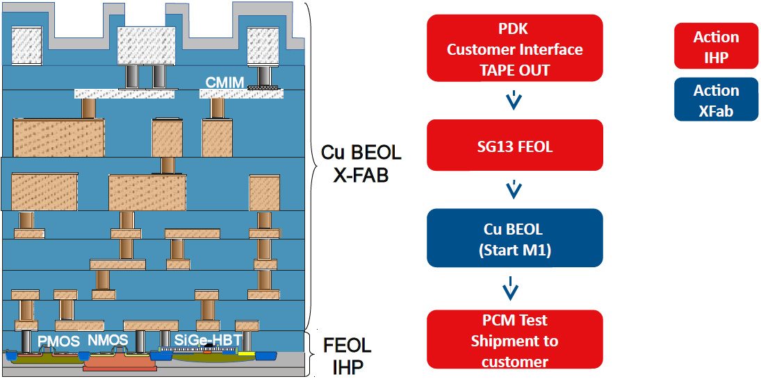
SG13SCu and SG13G2Cu: FEOL process SG13S and SG13G2 together with Cu BEOL option from XFAB containing 4 thin Cu layer, two 3μm Cu layer, a thin Al layer with 2 fF/μm MIM capacitor and a 2.8 μm Aluminum top layer.
Improvement of passive components compared to Al BEOL:
- 2 thick copper metal lines,
- higher current handling of thin metal layers
- higher current handling of the small vias
- 40% higher area density of MIM capacitor
SG13G3Cu technology offers IHP´s highest performance HBT’s with up to 470 GHz transit frequencies and up to 650 GHz maximum oscillation frequencies. The process offers a 8-layer Cu-BEOL from X-FAB containing 4 thin Cu layers, 2 thick 3μm Cu layers, a thin Al layer with 2 fF/μm MIM capacitor and a 2.8 μm Aluminum top layer. This technology offers CMOS devices with 130 nm gate length and 1.2 V core voltage and high voltage CMOS devices with 3.3 V core voltage.
SG25H5_EPIC technology is a high performance BiCMOS technology with integrated Silicon Photonic devices. It combines a BiCMOS process with very high bipolar performance 210 GHz transit frequencies and up to 280 GHz maximum oscillation frequencies and photonic devices from SG25_PIC.
Details on Photonic Integrated Circuit Module:
- 220 nm Si on 2 µm SiO2
- 3 etch depths
- 4 doping levels (p, n, p+, n+)
- 3 + 2 thick AI backend metal layers
- Germanium photo diodes (f3dB > 60 GHz)
- HBTs (fT/fmax = 220/290 GHz)
- optional localized backside etching
SG25H3 is a 0.25 μm BiCMOS technology with npn-HBTs that ranges from higher RF performance (fT/fmax = 110/180 GHz) to higher breakdown voltages up to 7 V.
SGB25V is a low cost BiCMOS technology with a range of npn-HBTs up to a breakdown voltage of 7 V.
SGB25RH is a special variant of SGB25V BiCMOS technology which includes radiation hard IPs for space applications. It is not allowed to use the radiation hard Process Design Kit IPs included here together with SGB25V technology.
A Cadence-based mixed signal Design Kit is available. For high frequency designs an analog Design Kit in Keysight ADS can be used. IHP's reusable blocks and IPs for wireless and broadband are offered to support your designs.
For details on the PDKs offered and the software supported refer to the design kit website:
Design Kit »
The following Modules are available:
LBE
The Localized Backside Etching module is offered to locally remove silicon to improve passive properties (available in all technologies).
PIC
Includes additional photonic design layers along with BiCMOS BEOL layers on SOI wafers.
TSV
Is an additional option in SG13S and SG13G2 technology that provides RF grounding by vias through silicon to improve RF performance.
- Through-Silicon Via Module for RF Grounding is available in SG13 technologies.
- Single TSVs can provide low GND industance ≈ 30 pH to improve RF circuit performance.
- Backside metallization can also be used for improved chip-to-package contacting.
MEMRES
MEMRES
- A fully CMOS integrated memristive module based on resistive TiN / HfO2-x / TiN switching devices in SG13S technology
- Process Design Kit including layout and VerilogA simulation model is also available