The main intention of heterogeneous integration is the realization of multifunctional microsystems with higher performance, increased functionality and smaller form factor.
The research group Heterointegration of Devices and Technologies (HDT) combines different disciplines and expertise starting from material and devices, FEM modelling & simulation in multi-physical domains as well as semiconductor and assembly technologies to develop new components and technology modules with a strong focus on high frequency applications.
Main targets
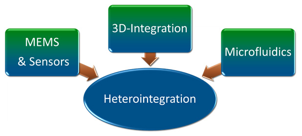
The research activities of HDT are mainly divided into three different pillars:
- integration of MEMS and sensors
- millimeter-wave wafer-level packaging and 3D integration
- microfluidics for millimeter-wave/ THz sensor technology
Research topics
- Si-based meta materials
- mm-wave module integration
- Wafer-to-Wafer bonding
- RF-module towards package integration
The research topic “MEMS & Sensors” includes the development of various types of microelectromechanical system (MEMS) components like high performance RF-MEMS switches/varactors as well as MEMS-based sensors like thermal detectors. RF-MEMS switches are embedded into IHP high performance SiGe BiCMOS technologies to minimize unwanted interconnection losses at very high frequencies making them promising for fully embedded switching/tuning solutions at mm-wave frequencies. MEMS technologies are also mandatory to realize a broad range of sensors, e.g. thermal detectors for infrared imaging applications. One of the main drivers for the integration of MEMS and sensors is the potential for high density integration of those MEMS-based components together with the read-out integrated circuits based on CMOS/BiCMOS technologies.
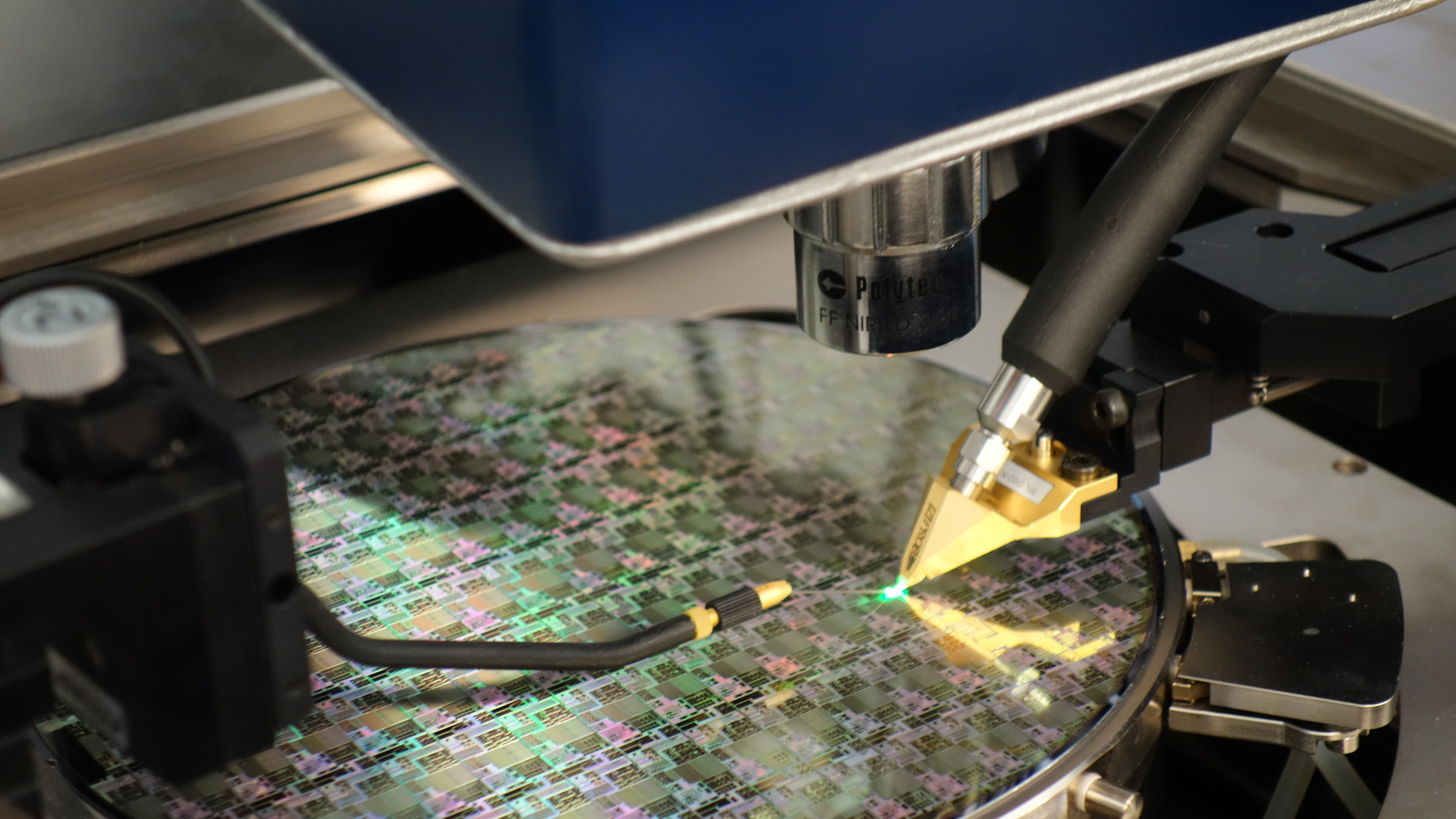
The research topic “3D Integration” covers a wide range of wafer-level packaging components and technologies, especially for high frequency applications. Nowadays wafer-level packaging and 2.5/3D integration are becoming the major drivers to fulfill the requirements for high performance multifunctional system integration. Through-Silicon Vias (TSV) are one example which enables 2.5/3D integration, e.g. to combine different ICs or different semiconductor technologies with high integration density and small form factor. Wafer-level packaging technologies are also under development to provide Fan-in and Fan-Out Wafer-level Packaging (FI/FO-WLP) of integrated circuits, which is one of the major requirements for high frequency packaging. Various techniques like interposer-based wafer-level packaging are under development to realize a 2.5/3D packaging platform for SiGe BiCMOS high frequency ICs. These interposers can also be useful to integrate high-Q passives and antenna-in-packages. One of the key enablers for 3D integration is a 200 mm wafer bonding pilot line including different temporary and permanent wafer bonding technologies within a clean room environment. Temporary wafer bonding is mainly applied as thin wafer handling whereas permanent wafer can be used e.g. for layer transfer and wafer-level interconnection technology.
The research topic “Microfluidics” comprises the development of a microfluidic platform based on IHP SiGe BiCMOS technology to enable biosensors and THz-sensing applications. BiCMOS embedded microfluidics enable small-size, low-cost and high reproducibility BiCMOS integrated microfluidic platforms for single-cell analysis and point-of-care diagnostics.
Research results
In recent years, the integration of different components and technology modules into IHP SiGe BiCMOS technologies has been successfully demonstrated for various applications. As an example high aspect ratio TSVs are integrated into IHP 130 nm SiGe BiCMOS technology SG13S/G2 as well as in silicon interposers, which can be applied for improved RF grounding of high frequency integrated circuits as well as 3D heterogeneous integration. The applicability of TSVs for the mm-wave and sub-THz frequency range has been demonstrated providing a very low insertion loss of less than 1 dB per TSV transition even up to 300 GHz. As a second example, a unique wafer-level packaging technology has been demonstrated which is based on a wafer-level Al-Al thermo-compression bonding process enabling fine pitch and reliable wafer-level interconnections. Electrical interconnections with very low parasitics can be achieved enabling mm-wave wafer-level interconnections with mΩ-range contact resistance and low transition loss. Finally high performance SiGe/Si multi-quantum well (MQW) based uncooled µ-bolometers have been demonstrated. Thermal detectors with very high temperature coefficient of resistance (TCR) values of > 5 %/K have been achieved. The integration of these thermal detectors together with the CMOS read-out circuit is done by a layer transfer technology based on low-temperature SiO2-SiO2 fusion bonding.