The process and device research group consists of around twenty experienced scientists (physicists, chemists) and engineers (electrical engineering, mechanical engineering).
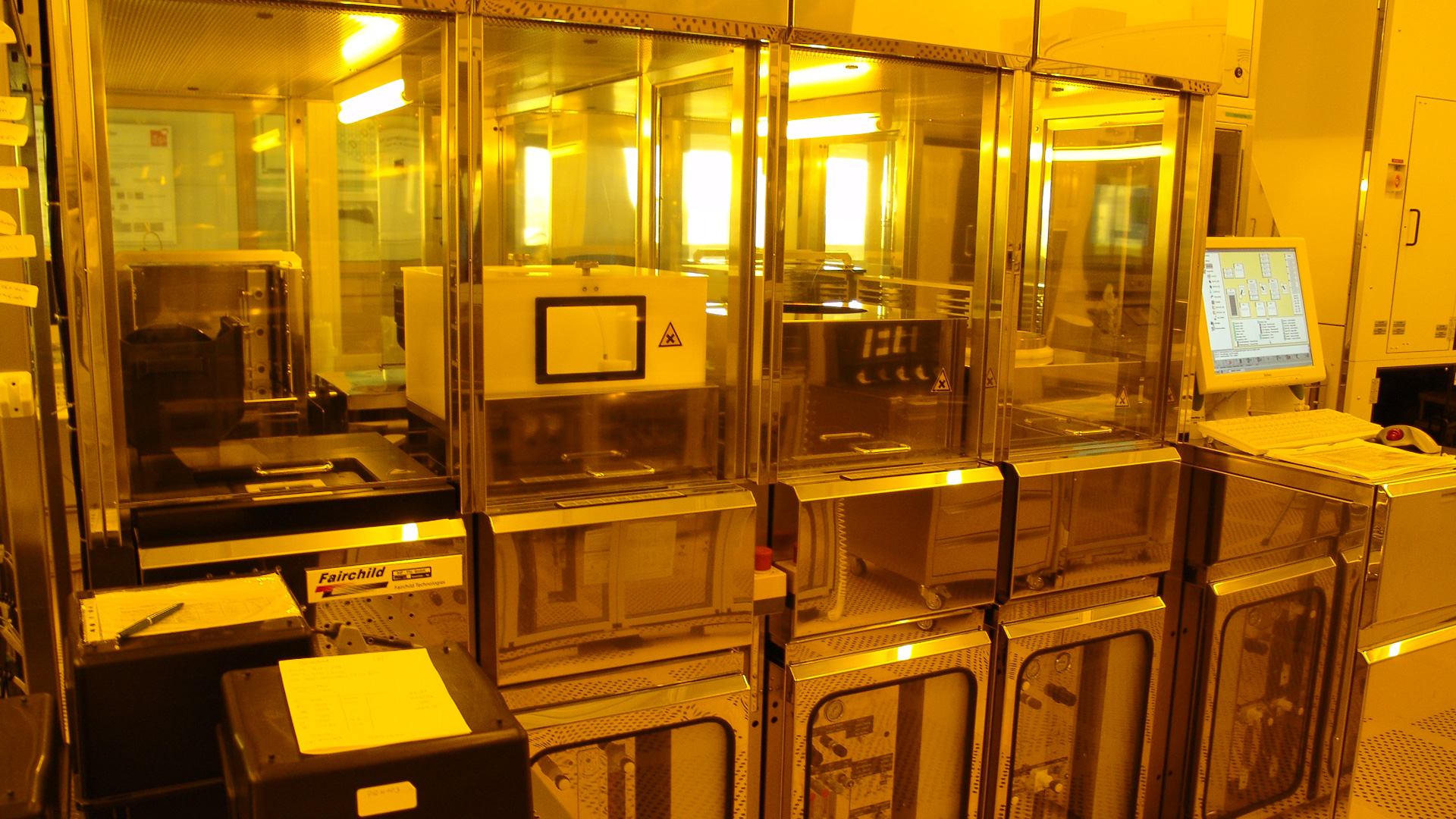
The working group is entrusted with the development of processes for the fabrication of the integrated circuits with the machine park in the cleanroom of the IHP. The cleanroom has a total usable area of 1500 m2, on which more than 40 fully automatic systems for semiconductor wafer processing are available. These are industry-compatible cluster tools and batch systems from renowned manufacturers exclusively for 200 mm wafers.
Main targets
The research group deals with the development of optimal recipes for the respective equipment and applications.
The process steps are:
- lithography
- ion implantation
- Rapid Thermal Processing (RTP)
- epitaxy
- thermal oxidation
- LPCVD
- PECVD
- ALD
- dry etching
- wet etching / cleaning
- metallization
- CMP
- inline measurement
Research topics
- providing of optimized processes for the development of the fastest HBT transistors and their integration into BiCMOS technologies
- development of processes for the integration of photonic components (waveguides, photodiodes) for the PIC and EPIC technologies
- development of process steps for integration concepts of III-V semiconductor materials such as InP, in particular to create new capabilities for the integration of these materials into the photonic processes
- integration of 2D materials such as graphene into industry-compatible Si technology processes
- optimization of passive devices such as thin film resistors and MIM capacitors in the metallization system of the integrated circuits
- integration of memristive devices for applications in machine learning and artificial intelligence
- generation and research of suitable layer systems for quantum computing
- SiGe-BiCMOS & devices for QT
- Si-process & emerging device developments
- fabrication of plasmonic structures
- fabrication of graphene-based devices
- fabrication and integration of memristive devices
- process development for quantum structures
Research results
The manufacturing processes in the cleanroom meet the high expectations in the development and stabilization of IHP technologies. The high yield in the qualified technologies is achieved through close cooperation with the other groups, such as electrical characterization, off-line characterization and of course process integration. Proof of this is the high scientific reputation of the IHP and the increasing number of customers for multi-project runs and small series production. In addition, there is the possibility of using the technology service, where the advanced capabilities of the IHP cleanroom with its process engineers are accessible in short runs.