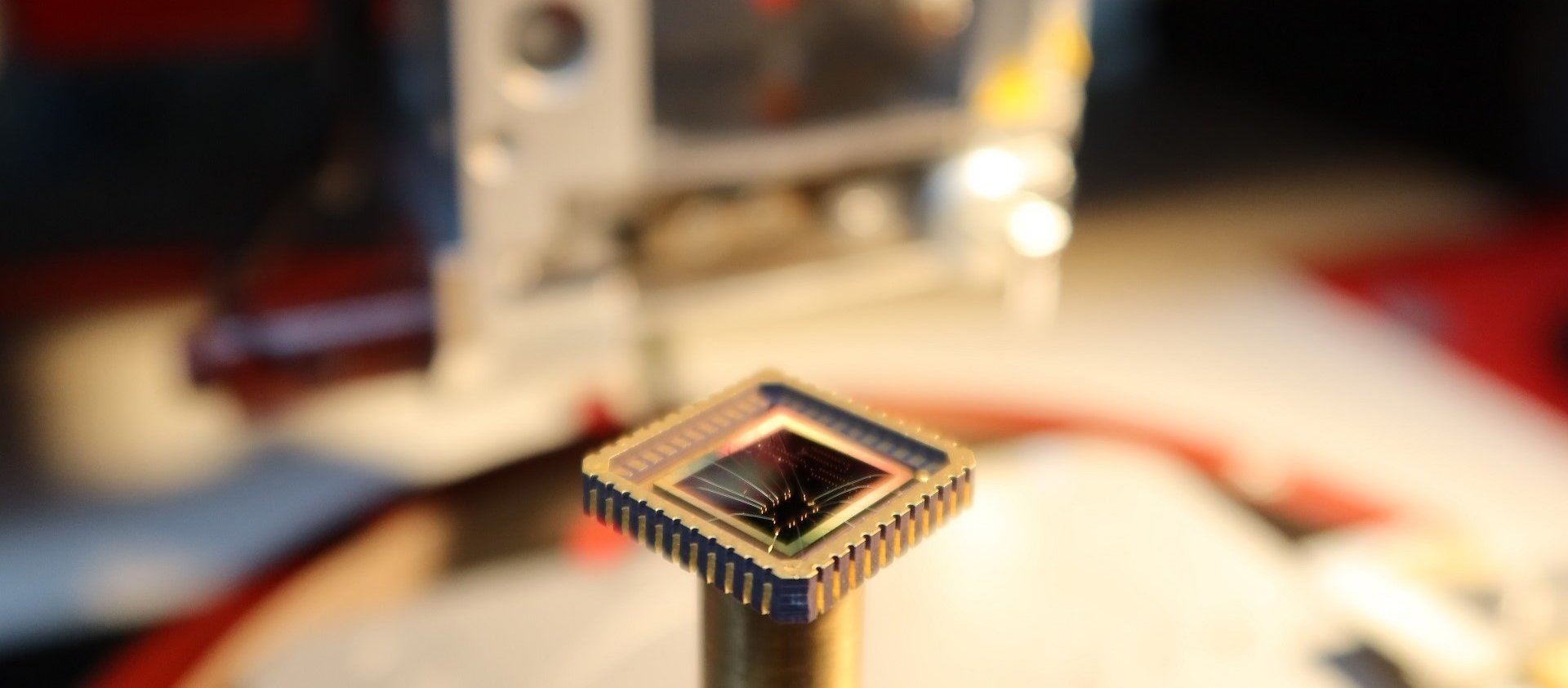
The Joint Lab Semiconductor-based Quantum Computing was founded in 2024 together with RWTH Aachen University and Forschungszentrum Jülich (FZ Jülich) as the next step in promoting academic and technological collaboration. Following a long-standing partnership, the Joint Lab is focussing on activities in the field of scalable quantum computer architectures and improvement of spin-based qubit and multi-qubit operations.
-
Research >> click here <<
Within ongoing third party funded projects, material research especially in group IV semiconductors aims for an established process line for quantum technology components. For this purpose, the necessary infrastructure for the production and characterisation of quantum devices is being established at IHP. A specially installed chemical vapour deposition (CVD) system enables the growth of isotope-pure SiGe quantum structures. First processed templates of silicon quantum wells have already been successfully tested. At IHP’s magneto transport laboratory which allows the characterization of devices at temperatures close to zero Kelvin and large magnetic fields, test devices have been characterized revealing top-notch charge carrier mobilities reflecting the high quality of the quantum wells, fabricated at IHP.
The Joint Lab's research focuses on:
- Development of the SiGe heterostructure to improve the material parameters, such as valley splitting and percolation threshold, and their local variation.
- Development of scalable quantum computer architectures with spin-based qubit and multi-qubit operations.
-
Projects >> click here <<
This research was supported by
- the Leibniz association "High-Definition Crystalline Silicon-Germanium structures for Quantum Circuits" project (SiGeQuant, Project No. K124/2018),
- the European Union and its Horizon 2020 framework program (Grant No. FETFLAG-05-2020) as part of the project "Quantum Large Scale Integration in Silicon" (QLSI, Grant No. 951852),
- and the German Federal Ministry of Education and Research within the frame of the project "Halbleiter-Quantenprozessor mit shuttlingbasierter skalierbarer Architektur" (QUASAR, FKZ Grant No. 13N15654).
-
Publications >> click here <<
- Local Laser-Induced Solid-Phase Recrystallization of Phosphorus-Implanted Si/SiGe Heterostructures for Contacts Below 4.2 K; M. Neul, I.V. Sprave, L.K. Diebel, L.G. Zinkl, F. Fuchs, Y. Yamamoto, C. Vedder, D. Bougeard, L.R. Schreiber; Physical Review Materials (2024)
- 200 mm Wafer Level Characterization at 2K of Si/SiGe Field-Effect Transistors; N.D. Komerički, P. Muster, F. Reichmann, T. Huckemann, D. Kaufmann, Y. Yamamoto, M. Lisker, W. Langheinrich, L.R. Schreiber, H. Bluhm, R. Quay; ECS Transactions (2024)
- Advancing Si Spin Qubit Research: Process Integration of Hall Bar FETs on Si/SiGe in a 200mm BiCMOS Pilot Line; F. Reichmann, A. Mistroni, Y. Yamamoto, P. Kulse, St. Marschmeyer, D. Wolansky, O. Fursenko, M.H. Zoellner, G. Capellini, L. Diebel, D. Bougeard, M. Lisker; ECS Transactions (2024)
- Fabrication of Gate Electrodes for Scalable Quantum Computing using CMOS Industry Compatible E-Beam Lithography and Numerical Simulation of the Resulting Quantum Device; V. Brackmann, M. Neul, M. Friedrich, W. Langheinrich, M. Simon, S. Pregl, A. Demmler, N. Hanisch, M. Lederer, K. Zimmermann, J. Klos, F. Reichmann, Y. Yamamoto, M. Wislicenus, C. Dahl, L. Schreiber, H. Bluhm, B. Lilienthal-Uhlig; Proc. 38th Mask and Lithography Conference (ELMC 2023), 12802, 128020F (2023)
- Lattice Deformation at the Submicron Scale: X-Ray Nanobeam Measurements of Elastic Strain in Electron Shuttling Devices2024/279a; C. Corley-Wiciak, M.H. Zoellner, I. Zaitsev, K. Anand, E. Zatterin, Y. Yamamoto, A.A. Corley-Wiciak, F. Reichmann, W. Langheinrich, L.R. Schreiber, C.L. Manganelli, M. Virgilio, C. Richter, G. Capellini; Physical Review Applied (2023)
- Nanoscale Mapping of the 3D Strain Tensor in a Germanium Quantum Well Hosting a Functional Spin Qubit Device; C. Corley-Wiciak, C. Richter, M.H. Zoellner, I. Zaitev, C.L. Manganelli, E. Zatterin, T.U. Schülli, A.A. Corley-Wiciak, J. Katzer, F. Reichmann, W.M. Klesse, N.W. Hendrickx, A. Sammak, M. Veldhorst, G. Scappucci, M. Virgilio, G. Capellini; ACS Applied Materials & Interfaces (2022)
- Role of Critical Thickness in SiGe/Si/SiGe Heterostructure Design for Qubits; Y. Liu, K.-P. Gradwohl, C.-H. Lu, T. Remmele, Y. Yamamoto, M.H. Zoellner, T. Schroeder, T. Boeck, H. Amari, C. Richter, M. Albrecht; Journal of Applied Physics (2022)
- Local Laser-Induced Solid-Phase Recrystallization of Phosphorus-Implanted Si/SiGe Heterostructures for Contacts Below 4.2 K; M. Neul, I.V. Sprave, L.K. Diebel, L.G. Zinkl, F. Fuchs, Y. Yamamoto, C. Vedder, D. Bougeard, L.R. Schreiber; Physical Review Materials (2024)


