IHP’s Technology department focuses on the development of devices, modules and technologies with specific properties for applications in communications, high-frequency electronics, sensor technologies and novel areas such as artificial intelligence and quantum technologies. The internal transfer of these developments to manufacturing in the own pilot line for IHP projects and for the worldwide MPW and prototyping service is another focus.
Research and development of the department consists of two main areas. One is the R&D of new devices, modules and technology platforms that are compatible with a Si-based process environment. The second area focuses on the transfer, optimization, stabilization and performance enhancement of existing IHP technologies. The goal is to offer selected modules and technologies to academic as well as to industrial partners within the IHP research service. The main focus of the work is the research and development of technology modules and integration concepts that can significantly enhance the functionality of CMOS technologies.
The strategic research topics are technologies with SiGe-based THz devices, Si/Ge photonic modules, devices for radiation-resistant applications and novel integration concepts, e.g. for high-frequency systems. In this context, the department pursues both monolithic and heterogeneous integration approaches. These approaches enable the combination of electronics with the functionality of the integrated modules on one chip. Applications for such technologies are especially in wireless, broadband and optical communication, in sensor technology and new fields of application such as artificial intelligence.
Considerable efforts are being made to qualify and expand the MPW and prototyping services based on the 0.25 µm and 0.13 µm technologies and to make them available to partners and customers worldwide.

Research, MPW & Prototyping Service
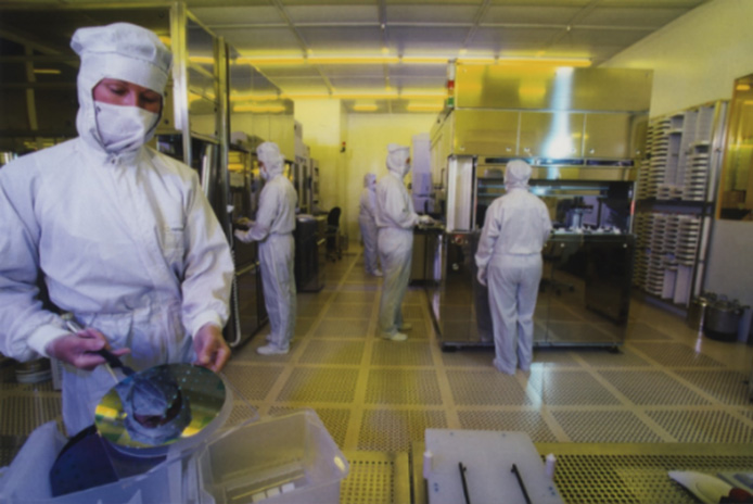
For more than 20 years, technological competence combined with curiosity for new developments has been the basis for continuous progress in the technology department of IHP, where about half of the institute's staff is employed, including those working in 24/7 clean room operation.
Technical Competencies
IHP is equipped with all the competencies necessary for developing and running world-class BiCMOS technologies:
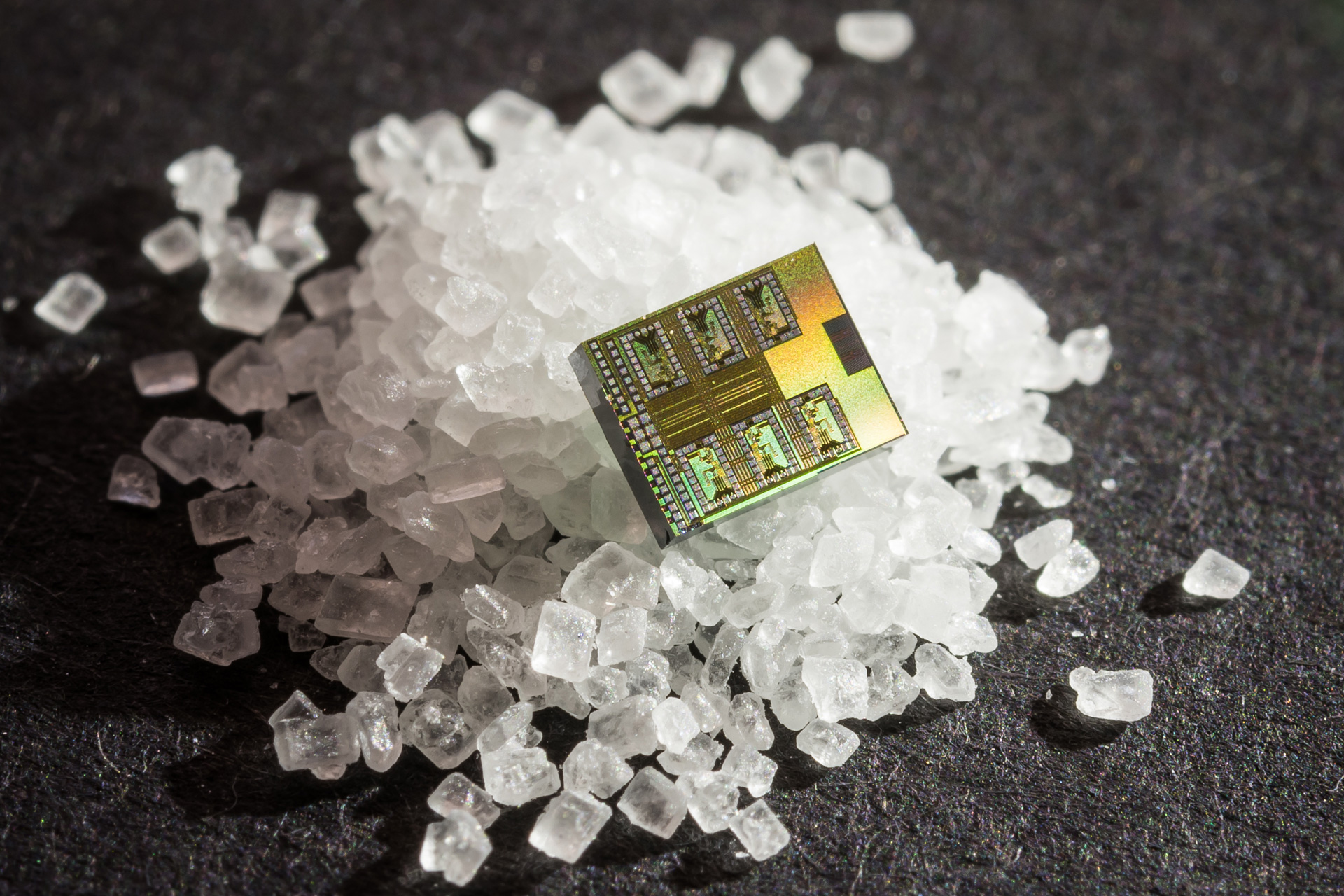
- SiGe:C HBTs and photonics modules (e.g. Ge-PD) and their integration into CMOS technologies
- modular extension of standard CMOS technologies
- process module and process step research and development
- electrical and opto-electrical measurements including RF tests
- diagnostic and analytical techniques necessary for developing and running technologies
- reliability and process qualification
- ensuring stable and reliable processes in the 24/7 operated CMOS-clean room
- research and module services as well as MPW and prototyping offerings for internal and external customers
- design kit support for internal and external projects
- transfer of technologies and technology modules from and to industrial partners
- integrating new materials into Si-based technologies
Technical Basis
The following methods are currently being used: