


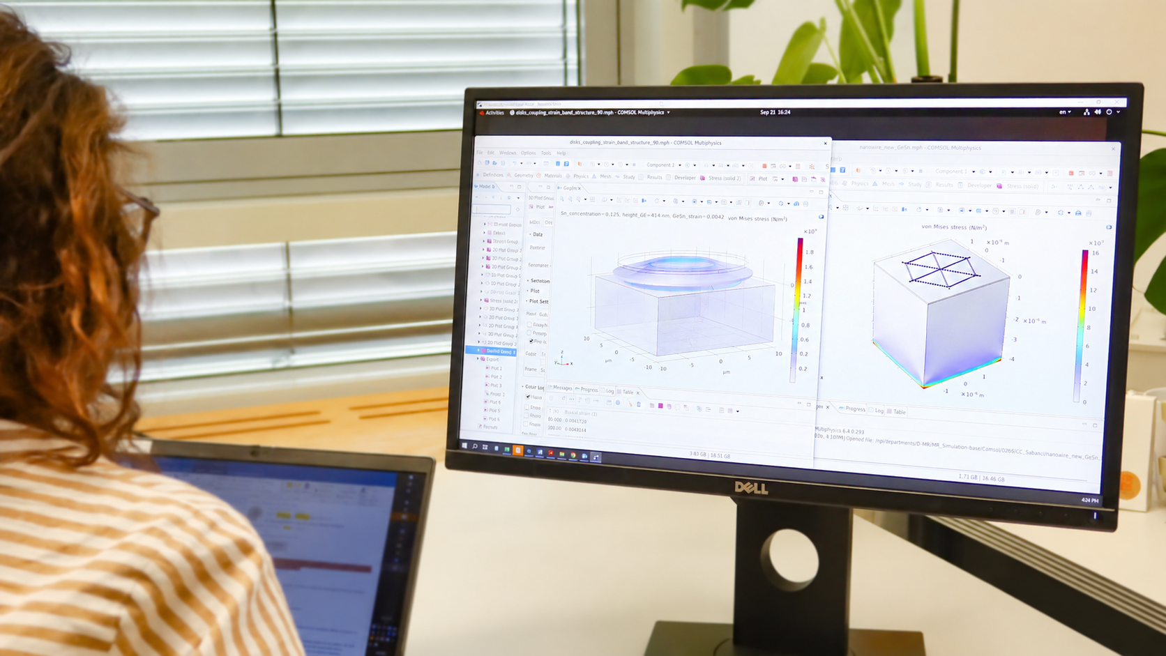
In this research group, we develop advanced modeling approaches for the design, understanding and optimization of semiconductor materials, heterostructures and devices. We combine material-level modeling with device-scale simulations, bridging fundamental material properties and the performance of emerging semiconductor technologies.
A central activity is the development of a unified modeling platform that integrates material parameters, experimental data and multiphysics simulations. The approach combines finite-element modeling with electronic and optical calculations to investigate strain, band structure, carrier behaviour, radiative recombination and heat transport in semiconductor structures. We follow FAIR data principles and is working towards increasingly interoperable and open modeling workflows.
Research relevance and application areas
Predictive materials modeling is becoming increasingly important as semiconductor technologies move towards complex material systems, nanoscale geometries and strongly coupled physical phenomena. Mechanical strain, temperature, composition and device geometry can simultaneously affect electronic and optical properties, making integrated multiphysics approaches essential for understanding and optimizing device performance.
The activities of the Computational Materials group support IHP’s research in photonics, quantum technologies, advanced microelectronics and energy-efficient devices. Particular emphasis is placed on Group IV semiconductor systems, including Si, Ge, SiGe, GeSn and SiGeSn. By closely connecting simulations with experimental characterization techniques such as X-ray diffraction (XRD), Raman spectroscopy and photoluminescence (PL), we provide a bridge between materials development, experimental characterization and predictive device design.
Main Research Objectives
- Develop integrated multiphysics modeling methodologies for advanced semiconductor materials and devices.
- Understand and exploit strain engineering as a tool to control the electronic and optical properties of Group IV semiconductor heterostructures.
- Predict band-structure modifications induced by strain, composition, geometry and temperature.
- Model coupled mechanical, thermal, electrical and optical phenomena from the material to the device scale.
- Develop modeling approaches for quantum-compatible semiconductor architectures, including strained quantum wells and gate-defined structures.
- Combine simulations with experimental characterization data to validate models and extract material parameters.
- Develop reusable and interoperable modeling workflows following FAIR data principles.
Research Areas
Strain engineering and Group IV materials
Finite-element modelling is used to investigate strain and strain-gradient distributions in Si, Ge, SiGe, GeSn and SiGeSn heterostructures and micro-/nanostructures. The simulations support the design of mechanically engineered materials for photonic, electronic and quantum applications and are closely correlated with structural characterization.
Electronic and band-structure modelling
We investigate the influence of strain, composition, temperature and geometry on semiconductor band structures and carrier confinement. Continuum approaches, deformation-potential models and advanced electronic-structure calculations are combined to connect mechanical deformation with electronic and optical properties.
Photonics and optoelectronic devices
Multiphysics simulations are applied to photonic and optoelectronic structures to study the interplay between mechanical deformation, temperature, optical properties and carrier recombination. Modelling activities are complemented by comparison with Raman and Photoluminescence.
Quantum semiconductor structures
We develop modeling approaches for semiconductor heterostructures relevant to quantum technologies, with particular emphasis on strained Si/SiGe quantum wells and gate-defined architectures. Mechanical simulations are coupled with electronic-structure and Schrödinger–Poisson calculations to investigate confinement, energy levels and strain-induced modifications of the electronic states.
Thermal and electro-thermal modelling
Thermal simulations are performed across material, heterostructure and device scales to investigate heat generation, transport and dissipation in advanced semiconductor technologies. Particular attention is devoted to coupled electro-thermal phenomena, including self-heating and the mutual interaction between temperature distributions and electrical device behaviour. These approaches are extended to quantum and cryogenic electronics on innovative material and devices.
Integrated Multiphysics Modelling
We provide the framework for connecting material parameters and different simulation levels within unified workflows. Commercial simulation environments are combined with internally developed numerical tools and experimental results to model coupled mechanical, thermal, electrical, electromagnetic and optical phenomena and to facilitate the transfer of material knowledge towards device design.

