


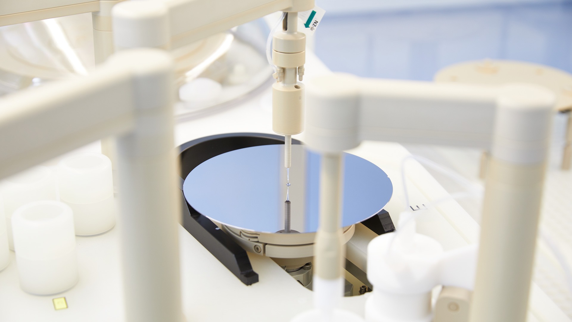
The Diagnostics, Sensors & Emerging Modules (DSE) research group combines process-oriented semiconductor analysis and failure diagnostics with the development of photonic sensor concepts and emerging technology modules. Through its two complementary teams, Material Analysis and Metrology (MAM) and Device and Module Development (DMD), the group operates at the interfaces between materials, processes, devices and applications.
Together with companies—particularly small and medium-sized enterprises (SMEs)—and scientific partners, we develop application-specific analysis methods, cleanroom process flows and demonstrators. A particular strength of DSE is its ability to combine expertise ranging from materials and device analysis to photonic sensing and technological integration. This enables us to assess new ideas at an early stage, investigate their technical feasibility and transfer promising approaches into collaborative research, innovation and technology-transfer activities.
Research Relevance and Application Areas
The increasing complexity of semiconductor materials, process structures and integrated electronic-photonic systems requires advanced analysis methods and an in-depth physical understanding of the resulting measurement data. DSE supports the development and optimisation of semiconductor processes, the qualification of technologies and equipment, and the localisation and root-cause analysis of failures. Further application areas include photonic sensing and biosensing, trustworthy electronics, backside technologies, and the integration of sensitive or biofunctionalised devices under gentle process conditions.
DSE provides SMEs in particular with access to specialised analytical infrastructure and interdisciplinary technology expertise. Technological challenges can initially be assessed through feasibility studies and subsequently developed into joint research or technology-transfer projects. Beyond its own research activities, DSE initiates and coordinates interdisciplinary research and innovation consortia, brings together complementary partners from industry and academia, and contributes the group’s expertise where it creates particular value for the overall project. Close collaboration with other IHP research groups and service units enables successful approaches to be transferred into prototyping, service and technology-transfer pathways.
Main Research Objectives
Material Analysis and Metrology (MAM)
- Advancing materials analysis, metrology and failure-diagnostics methods for semiconductor materials, process structures, devices and modules
- Developing new analysis methods and designed-in test concepts for photonic devices and integrated electronic-photonic systems
- Supporting process development and the qualification of technologies and equipment through quantitative materials and structural analysis
- Developing application-specific preparation, measurement and analysis workflows, including the scientific interpretation of complex measurement data
Device and Module Development (DMD)
- Developing photonic sensor concepts and devices, particularly for biosensing applications
- Developing and optimising application-specific cleanroom process flows
- Advancing local backside release and local backside etching processes
- Applying low-temperature integration concepts, such as NanoWiring, to sensitive and biofunctionalised devices
Cross-Cutting Objectives
- Developing controlled backside access and backside thinning processes for advanced analysis applications
- Investigating active backside protection concepts for trustworthy electronics
- Transferring exploratory technology concepts into feasibility studies and application-oriented demonstrators
- Integrating emerging technology concepts into interdisciplinary research and technology-transfer consortia
Research Areas
Materials Analysis, Metrology and Failure Analysis
The Material Analysis and Metrology team characterises semiconductor materials, thin films, process structures and microelectronic devices. It supports internal and external partners in process and failure analysis and in identifying and scientifically evaluating the underlying physical and chemical causes. MAM therefore makes an essential contribution to process development, process control, technology qualification and failure diagnostics. Its analytical methods are also used to qualify process equipment following new installations, process modifications or maintenance activities.
The team investigates surface topographies and layer structures, material composition and stoichiometry, as well as dopant concentrations and depth profiles. Structural and construction analyses also enable the assessment of geometries, material combinations and manufacturing characteristics of microelectronic devices.
A broad range of complementary methods is available, including scanning electron microscopy (SEM), transmission electron microscopy (TEM), focused ion beam analysis and preparation (FIB), Auger electron spectroscopy (AES), X-ray photoelectron spectroscopy (XPS), time-of-flight secondary ion mass spectrometry (ToF-SIMS), dynamic secondary ion mass spectrometry (D-SIMS), and photonic and laser-based methods for fault localisation.
The team’s work extends beyond individual measurements. MAM develops application-specific preparation, measurement and analysis workflows, adapts methods to new materials and devices, and provides the scientific interpretation of complex measurement data, spectra, depth profiles and microscopic findings.
Analysis Methods for Photonic Devices
A strategic focus of the DSE research group is the development of new analysis and diagnostic methods for photonic devices and integrated electronic-photonic systems. While photonic and laser-based techniques can also be used to localise faults in electronic circuits, this research area focuses on analysing the photonic device itself.
DSE develops complete analysis workflows, ranging from the definition of suitable measurement parameters and test structures to electrical and optical characterisation, fault localisation and physical root-cause analysis. Designed-in test concepts are a particular area of development. In these concepts, analysis and diagnostic capabilities are already considered during the design of a photonic device. This allows process deviations, faults and performance limitations to be localised and understood more effectively at later stages.
Photonic Devices and Biosensing
The Device and Module Development team develops photonic sensor concepts, devices and application-specific technology modules. Photonic biosensing is a particular focus.
For these applications, DMD develops suitable cleanroom process flows and uses and advances IHP’s established local backside release and local backside etching processes. These processes provide targeted backside access to the active photonic sensing area, while optical and electrical connections on the front side remain available for subsequent system integration.
DSE combines device development, cleanroom processing, characterisation and analysis to advance new sensor concepts towards application-oriented demonstrators.
Technology-transfer example: photonic biosensor demonstrator
Together with HyPhoX and within the Joint Lab operated by IHP and the Technical University of Applied Sciences Wildau, photonic sensor and integration concepts are being developed into system-level demonstrators. A mobile biosensor platform presented within this collaboration combines optical, electronic, microfluidic and biochemical functions in a compact analytical system. The platform addresses the rapid detection of biological targets in liquids, with potential applications in medical diagnostics, food analysis, environmental monitoring and industrial process control.
Further information: HyPhoX and the photonic biosensor demonstrator
Selected publications
- CMOS-Compatible Silicon Photonic Sensor for Refractive Index Sensing Using Local Back-Side Release, IEEE Photonics Technology Letters, 2020. DOI: 10.1109/LPT.2020.3019114
- Back-Side Release of Slot Waveguides for the Integration of Functional Materials in a Silicon Photonic Technology With a Full BEOL, IEEE Transactions on Components, Packaging and Manufacturing Technology, 2020. DOI: 10.1109/TCPMT.2020.3011149
- Optimization of Local Backside Released Micro-Ring Resonators for Sensing Applications Using Silicon Photonic Integrated Circuits in an SOI Technology, Proceedings of SPIE, 2025. DOI: 10.1117/12.3056481
Backside Technologies and Trustworthy Electronics
DSE develops processes for controlled access to the backside of integrated circuits. These include application-specific preparation workflows and the local or full-area backside thinning of individual chips for subsequent analytical procedures.
An IHP-developed method uses a material-selective process stop to thin integrated circuits in a controlled manner to a level immediately adjacent to the active device layer, while preserving their functionality for subsequent investigations.
Further information: International patent application WO2025088095A1 – Method and device for backside thinning of an integrated circuit
Building on its expertise in photonic devices, backside processing and system integration, DSE also investigates active backside protection concepts for security-critical semiconductor chips. A patented architecture uses integrated light emitters and detectors to identify changes within an interconnected protection and circuit system. The technological implementation and development of the required cleanroom processes are currently at an early stage of research and development.
Further information: European patent EP4086950B1 – Semiconductor device with backside protection mechanism
Low-Temperature Integration of Sensitive Devices
A further development area is the use of gentle integration and interconnection methods for temperature-sensitive and biofunctionalised devices and sensors. DSE investigates, among other approaches, nanowire-based interconnection technologies such as NanoWiring.
DSE focuses on the application-specific adaptation and use of these interconnection technologies for sensitive sensors and devices. The aim is to integrate them into functional modules and demonstrators with minimal thermal and mechanical stress. This work is carried out in close cooperation with the responsible integration groups at IHP and with external technology partners.
Contact us if you would like to jointly assess a technological challenge, develop a feasibility study, or initiate a collaborative research or technology-transfer activity.