



IHP gives researchers and development teams access to high-performance SiGe BiCMOS and silicon photonics technologies for advanced RF, mmWave, mixed-signal and photonic ICs. The broader Multi-Project Wafer (MPW) service uses 200 mm/8-inch silicon wafers.
Through our MPW and prototyping services, you can validate new chip designs using established 0.13 µm and 0.25 µm technology platforms, including HBT performance up to 650 GHz fmax without the cost of a dedicated wafer run.
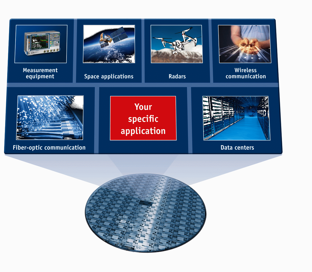
The standard 0.13 and 0.25 μm CMOS processes provide NMOS, PMOS, isolated NMOS and passive components such as poly resistors and MIM capacitors. In addition to the standard processes, we cover various front-end-of-line options, including an enhanced BEOL option with copper.
For a complete overview of technologies and shipping dates, please check the MPW Schedule and Price Information.
Design and fabrication
Design kits for Cadence and Keysight ADS support the development process from circuit design through prototyping and towards low-volume production.
We provide
- a Cadence-based mixed-signal Design Kit;
- a Keysight ADS analog Design Kit for high-frequency design;
- reusable wireless and broadband IP/blocks;
- PDK support for specialized modules.
Core SiGe BiCMOS and Silicon Photonics Technologies
0.13 μm CMOS Al-Backend: five thin and two thick Top Metal (TM) layers: TM1 – 2 μm, TM2 – 3 μm.
The SG13G3Cu technology offers IHP´s highest performance HBT’s with up to 500 GHz transit frequencies and up to 650 GHz maximum oscillation frequencies. The process offers an 8-layer Cu-BEOL from X-FAB containing thin Cu layers, 2 thick Cu layers, a thin Al layer with 2 fF/μm MIM capacitor and a thick Aluminum top layer. This technology offers CMOS devices with 130 nm gate length and 1.2 V core voltage and high voltage CMOS devices with 3.3 V core voltage.
Customers can extend the base processes with the following specialized modules:
- LBE (Localized Backside Etching)
- H7PIC
- MEMRES
- TSV
For more details on the PDKs offered and the software supported, refer to the design kit page.
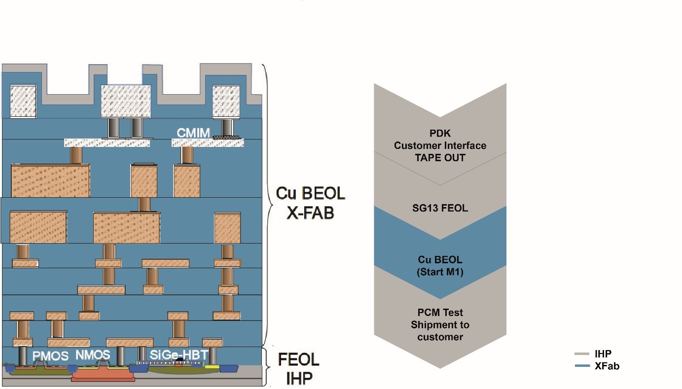
SG13G2Cu: FEOL process SG13G2 together with Cu BEOL option from XFAB containing 4 thin Cu layer, two thick Cu layers, a thin Al layer with 2 fF/μm MIM capacitor and a thick Aluminum top layer.
Improvement of passive components compared to Al BEOL:
- 2 thick copper metal lines,
- 10 times higher current handling of thin metal layers and small vias
- 40% higher area density of MIM capacitor
Silicon Photonic processes
Standard backend: three thin metal layers and two Top Metal (TM) layers: TM1 – 2 μm, TM2 – 3 μm.
SG25H7_EPIC
Main capability: CMOS + Silicon Photonics
SG25H7_EPIC is a monolithic photonic BiCMOS technology comprising npn HBTs with fT / fmax = >350/>500 GHz, Ge-fin photodiodes with f3dB >110 GHz, and full photonic device set for C/O-band
Details on the Photonic Integrated Circuit Module:
- 220 nm Si on 2 µm SiO2
- 3 etch depths
- 4 doping levels (p, n, p+, n+)
- 3 + 2 thick AI backend metal layers
- Germanium photo diodes (f3dB >110 GHz)
- HBTs (fT / fmax = >350/>500 GHz)