


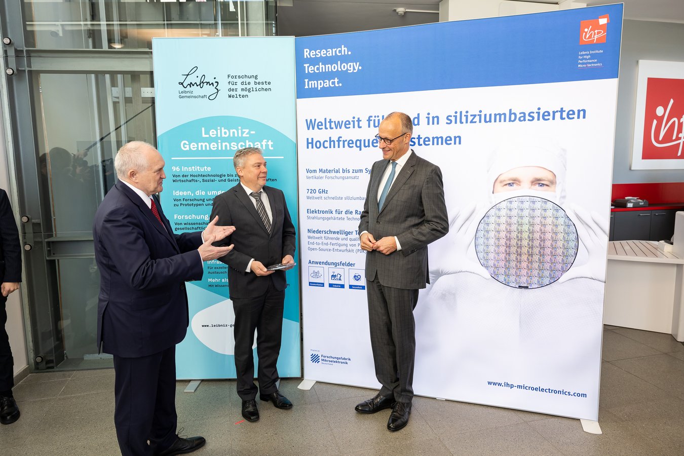
Today, Federal Chancellor Friedrich Merz visited IHP – Leibniz Institute for High Performance Microelectronics in Frankfurt (Oder). The visit highlighted the strategic importance of semiconductor research for Germany’s technological sovereignty, innovative capacity and economic competitiveness. The visit, which took place at the invitation of the Leibniz Association, focused on the contribution of the Leibniz Association, and IHP in particular, to Germany’s High-Tech Agenda, in which the Federal Government identifies microelectronics as one of six key technologies.
The Federal Chancellor was accompanied by Dr Marcus Pleyer, State Secretary at the Federal Ministry of Research, Technology and Space, and Tobias Dünow, State Secretary at the Brandenburg Ministry of Science, Research and Culture. Prof. Dr. Dr. h. c. Christoph M. Schmidt, President of the Leibniz Association, and Prof. Dr.-Ing. Gerhard Kahmen, Scientific and Technical Director of IHP, guided him through the institute. He toured the institute’s cleanroom and high-frequency measurement laboratory and viewed research demonstrators showcasing communication and sensing technologies for the next generation of mobile communications, 6G, as well as photonic biosensors for rapid diagnostics.
Microelectronics: A Strategic Capability for Germany and Europe
“Microelectronics is a key technology for the sovereignty of Germany and Europe,” says Prof. Gerhard Kahmen. “At IHP, we make our research results available to partners in academia and industry not only as laboratory samples, but also in the form of qualified prototypes and small production runs.”
As a research institute specialising in silicon-based microelectronics, IHP contributes to these objectives by combining fundamental research, technology development, semiconductor manufacturing and system validation. Following the Lab-to-Industry principle, IHP’s integrated research infrastructure enables technologies to be developed and tested across the entire value chain.
IHP’s semiconductor pilot line in Frankfurt (Oder) plays a central role in this process. The institute operates the only end-to-end production line at a research institution in Europe capable of manufacturing silicon-germanium BiCMOS technologies (SiGe BiCMOS) and electronic-photonic integrated circuits (EPICs) under near-industrial conditions.
From 6G Networks to Lab-on-a-Chip
One of the projects presented during the visit was an intelligent wireless communication system for the next generation of mobile networks. IHP researchers have developed a demonstrator that operates in real time at 60 GHz, combining high-speed data transmission with sensing of its surroundings. Using the same signal and hardware, the system can simultaneously transmit information and detect objects or people in its environment.
This technology, known as Integrated Communications and Sensing (ICAS), is considered a key feature of future 6G networks. Potential applications range from monitoring industrial environments and detecting drones near critical infrastructure to contactless sensing technologies for healthcare. IHP developed the demonstrator as part of the Open6GHub 6G research consortium, funded by the Federal Ministry of Research, Technology and Space (BMFTR).
A second example demonstrated how semiconductor research can lead to new products and companies. HyPhoX GmbH, a joint spin-off from the Joint Lab of IHP and the Technical University of Applied Sciences Wildau (TH Wildau), together with the Federal Institute for Materials Research and Testing (BAM), is developing miniaturised photonic biosensors that deliver quantitative measurements within minutes. The company was founded with funding from the Federal Government’s EXIST start-up programme. Its technology combines microelectronics, photonics and biochemistry on a sensor chip measuring just 2 mm².
Manufactured using standard processes on IHP’s pilot line, these chips could enable the future use of portable testing systems for medical diagnostics, water quality testing, food safety and environmental monitoring. The company demonstrates how publicly funded research can generate economic value.
Infrastructure for Technological Sovereignty
The Federal Chancellor also toured IHP’s cleanroom, including its pilot line, and the high-frequency measurement laboratory.
By developing technological capabilities and strengthening strategic supply chains, IHP contributes to the resilience of German and European industry. Its cleanroom provides the facilities to develop, manufacture and validate SiGe BiCMOS technologies under near-industrial conditions. The facility supports scientific research, open silicon technologies and industrial customers seeking to have chips manufactured based on their own designs. Operating around the clock, the cleanroom comprises 1,500 m² of ISO Class 3 cleanroom space in accordance with DIN EN ISO 14644-1 for processing 200 mm silicon wafers using 0.13 µm technology. A further 300 m² is dedicated to wafer bonding and the heterogeneous integration of chiplets.
In its high-frequency laboratory, IHP tests and characterises circuits manufactured in its own cleanroom for wireless communications, sensing and radar applications. Broadband measurements from 0 to 250 GHz can be performed using a single measurement probe—a capability currently unique in Germany. IHP’s expertise is also demonstrated by its world record for the oscillation frequency of silicon-based transistors, at 720 GHz.
The Federal Chancellor’s visit highlighted the role of the Leibniz Association and its research institutions in implementing Germany’s High-Tech Agenda. By combining scientific expertise, specialised infrastructure, technology development and knowledge transfer, IHP and the institutes of the Leibniz Association help strengthen the technological capabilities of Germany and Europe.
