
Progress in work on memristive circuits and systems is growing rapidly. They find applications in non-volatile memories, advanced computing technologies, e. g. edge AI computing applications, or in hardware artificial neural networks (ANNs) with memristive elements as synaptic elements. The electrical characteristics of memristive cells enable modeling of synaptic weights of neuronal synapses and implementation of neural network architectures. Meanwhile, memristive device-based approaches to neuromorphic chips are widely investigated, revealing also challenges, such as the variability of switching parameters and the energy costs associated with analog-to-digital and digital-to-analog conversion. Addressing these challenges will be now possible with the latest offering in IHP's Multi Project Wafer Service. IHP offers a fully CMOS integrated memristive module (MEMRES) based on resistive TiN / HfO2-x / TiN switching devices in its SG13S technology, along with a Process Design Kit including layout and VerilogA simulation model.
By providing the MEMRES module the IHP gives circuit designers around the world the opportunity to create neuromorphic circuits with integrated memristive technologies in the near future. “Thanks to IHP's memristive devices in its 130 nm technology, we were able to successfully participate in the BMBF-funded call for proposals Energy-efficient AI system and to achieve first place with our project Lo3-ML. Based on our positive experiences, we will also rely on IHP's semiconductor competence and especially on the memristive devices in the planned follow-up project and use them for the design of energy-efficient circuits with non-volatile memory elements.”, says Dr. Marc Reichenbach from Friedrich–Alexander University Erlangen–Nürnberg.
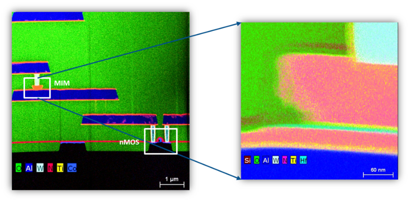
The memristive module MEMRES consists of 18 additional steps and is integrated into the standard back end of line of the 130 nm CMOS process of IHP. It is fabricated between the Metal 2 and Metal 3 Layers. The module consists of a Metal-Insulator-Metal (MIM) stack. Patterning of the MIM stack is one of the crucial steps in the MEMRES fabrication process. Hence, the devices are patterned with improved fabrication technique consisting of a spacer and encapsulation process steps. Further, different memristive switching layers like HfO2 and Al2O3 are used in combination to obtain analog switching behavior which is crucial for the neuromorphic computing applications.
