
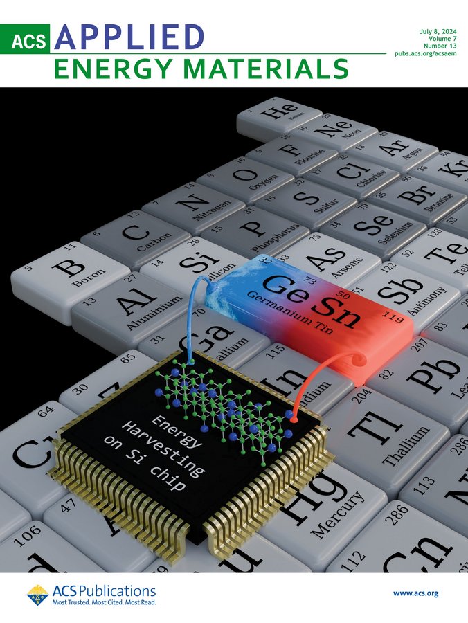
Researchers from Germany, Italy, and the UK have achieved a major advance in the development of materials suitable for on-chip energy harvesting. By composing an alloy made of silicon, germanium and tin, they were able to create a thermoelectric material, promising to transform the waste heat of computer processors back into electricity. With all elements coming from the 4th main group of the periodic table, these new semiconductor alloy can be easily integrated into the CMOS process of chip production. The research findings made it onto the cover of the renowned scientific journal ACS Applied Energy Materials.
The increasing use of electronic devices in all aspects of our lives is driving up energy consumption. Most of this energy is dissipated into the environment in the form of heat. In Europe, about 1.2 Exajoule of low-temperature heat is wasted from IT infrastructures and devices, such as data centers and smart devices, per year. This is roughly equivalent to the primary energy consumption of Austria or Romania. This low-grade heat below 80°C is traditionally challenging to harness due to poor thermodynamic efficiency and technological constraints.
Therefore, utilizing the low-temperature heat directly for computer processors seems to be an ideal solution. But there are only very few materials available to convert the heat into electrical energy, and none of them are compatible with current technology in semiconductor fabrication plants.
A research collaboration between Forschungszentrum Jülich and IHP – Leibniz Institute for High Performance Microelectronics in Germany, together with the University of Pisa, the University of Bologna in Italy, and the University of Leeds in the UK, now reached a milestone in developing suitable materials for on-chip energy harvesting that are compatible with the CMOS process of chip production.
"Adding tin to germanium significantly reduces the material’s thermal conductivity while maintaining its electrical properties, an ideal combination for thermoelectric applications", explains Dr. Dan Buca, leader of the research group at Forschungszentrum Jülich. The experimental confirmation of the low lattice thermal conductivity, published in ACS Applied Energy Materials, highlights the great potential of these GeSn alloys as thermoelectric materials. The idea behind this: By integrating these alloys into silicon-based computer chips, it is possible to utilise the waste heat generated during operation and convert it back into electrical energy. This on-chip energy harvesting could significantly reduce the need for external cooling and power, leading to more sustainable and efficient IT devices.
In addition, Group IV elements, also known as the silicon group, form the basis of any electronic device, and by exploiting their alloying properties, the application areas are now expanding to include thermoelectrics, photonics and spintronics. The monolithic integration of photonics, electronics and thermoelectrics on the same chip is the ambitious long-term goal of silicon based technology. By combining these fields, it is possible not only to improve the performance of devices, but also to support the development of more sustainable technologies.
“In the paper we made a very important step. We have evaluated one of the most critical parameters for a thermoelectric material, the thermal conductivity, using a suite of different experimental techniques on epitaxial samples with different alloy compositions and thicknesses”, says Prof. Giovanni Capellini, project leader at IHP. "Our joint research can have a sizeable impact in the field of ′Green IT′ infrastructures. "
The research groups at Forschungszentrum Jülich and IHP are continuing their successful collaboration. They aim to further develop the material by extending the alloy composition to SiGeSn and the ultimate Group IV alloy CSiGeSn, and to fabricate a functional thermoelectric device to demonstrate the energy harvesting potential of Group IV alloys. The activity is financially supported by a newly awarded DFG grant "SiGeSn alloys for energy harvesting at room temperature". In addition, this activity for FZJ is partially supported by the Board of Directors via the collaborative PhD project "CMOS energy harvesting for big data applications".
More about thermoelectric elements:
A thermoelectric element converts temperature differences directly into electrical energy. When there is a temperature gradient across a thermoelectric material, it induces a flow of charge carriers, generating electricity. This process can be used to capture and recycle waste heat in electronic devices, converting it back into usable energy and reducing overall energy consumption.
For thermoelectric materials, lower thermal conductivity is desirable because it allows for a greater temperature gradient, which is essential for efficient energy conversion. GeSn alloys, with their reduced thermal conductivity, excel in creating this gradient, enhancing their thermoelectric performance.
More about the paper:
The current issue:
