The research group deals with research on new device concepts and fabrication technologies for Si-based integrated circuits. We develop high-frequency SiGe BiCMOS technologies as well as extensions of these platforms to new application areas such as electro-optical integrated circuits.
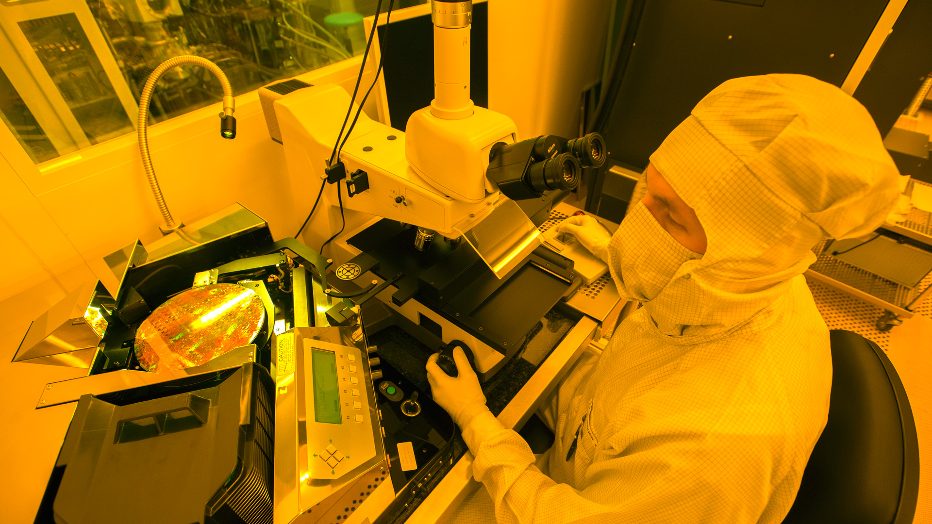
A team of experienced scientists, engineers and technicians work, in addition to our clean room, in laboratories with excellent equipment on an area of more than 250 m2. The 13 half and fully automatic 200 mm and 300 mm probing stations in the labs enable a rapid, flexible and efficient electrical on-wafer characterization level for our internal and external project partners.
Main targets for Technology Development
- Si-based process technologies for RF, THz, and optoelectronic applications
- high-speed SiGe heterojunction bipolar transistors (HBT)
- BiCMOS integration
- integration of optical components in SiGe-BiCMOS
Main targets of Electrical Characterization
Development and maintenance of necessary capabilities for electrical characterization of IHP SiGe:C BiCMOS and EPIC technologies, including process monitoring and control, device modelling, RF characterization, ESD testing, mixed-signal circuit testing and radiation hardness testing. Comprehensive on-wafer characterization of devices and circuits for development and qualification of innovative technologies.
- DC/CV parameter testing in the cleanroom and in the lab
- mixed-signal and radiation hardness testing of prototype devices
- S-Parameter, RF noise, LF noise
- optical and electrical characterization with full photonic device set for C/O-band
- improvement of radiation tolerance for integrated MOS and RF LDMOS transistors
Research topics
- SiGe-BiCMOS technologies
- SiGe-BiCMOS for space
- SiGe-HBT and BiCMOS for communication
- yield enhancement and technology optimization
- SiGe-HBT and RF device developments
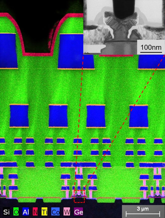
A major focus of the group is the development of high-speed SiGe BiCMOS technologies and their characterization. These activities reach from basic device research to qualification of fabrication processes according to industry standards. Current research activities are directed towards SiGe HBTs with maximum oscillation frequencies of 0.7 THz. A further research area is the development of technologies for high-speed electronic-photonic integrated circuits. This includes the integration of optical functions such as waveguides, photo diodes, and electro-optical modulators in SiGe BiCMOS technologies.
Research results
Several generations of high-speed SiGe HBTs have been developed and integrated in BiCMOS technologies which are available for chip fabrication via IHP’s MPW and prototyping service. The 130 nm BiCMOS process SG13G2 represents the fastest currently available SiGe HBT technology featuring peak fT/fmax values of 350 GHz/450 GHz. These developments are based on a series of pioneering contributions to SiGe HBTs technology including the use of carbon doping as a performance booster and the development of HBT architectures with low-resistive epitaxial base links for highest RF-performance. Within the joint European research projects DOTFIVE and DOTSEVEN, we have demonstrated for the first time SiGe HBTs with maximum oscillation frequencies of 500 GHz and 700 GHz, respectively. Current research projects address the integration of the latest HBT generation in the 130 nm BiCMOS technology platform.